Datasheet 搜索 > 计数器 > ON Semiconductor(安森美) > MC74HC589ADR2 数据手册 > MC74HC589ADR2 其他数据使用手册 1/13 页

 器件3D模型
¥ 0.497
MC74HC589ADR2 其他数据使用手册 - ON Semiconductor(安森美)
制造商:
ON Semiconductor(安森美)
分类:
计数器
封装:
SOIC-16
描述:
8位串行或并行输入/串行输出移位寄存器具有三态输出 8-Bit Serial or Parallel-Input/Serial-Output Shift Register with 3-State Output
Pictures:
3D模型
符号图
焊盘图
引脚图
产品图
页面导航:
引脚图在P1P7Hot
典型应用电路图在P1
封装尺寸在P11P12
焊盘布局在P11P12
型号编码规则在P1P10P12
标记信息在P1P12
封装信息在P10
技术参数、封装参数在P10
应用领域在P1P10
电气规格在P3P4
型号编号列表在P2
导航目录
MC74HC589ADR2数据手册
Page:
of 13 Go
若手册格式错乱,请下载阅览PDF原文件
© Semiconductor Components Industries, LLC, 2014
August, 2014 − Rev. 7
1 Publication Order Number:
MC74HC589A/D
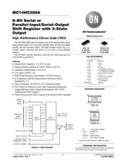
MC74HC589A
8-Bit Serial or
Parallel-Input/Serial-Output
Shift Register with 3-State
Output
High−Performance Silicon−Gate CMOS
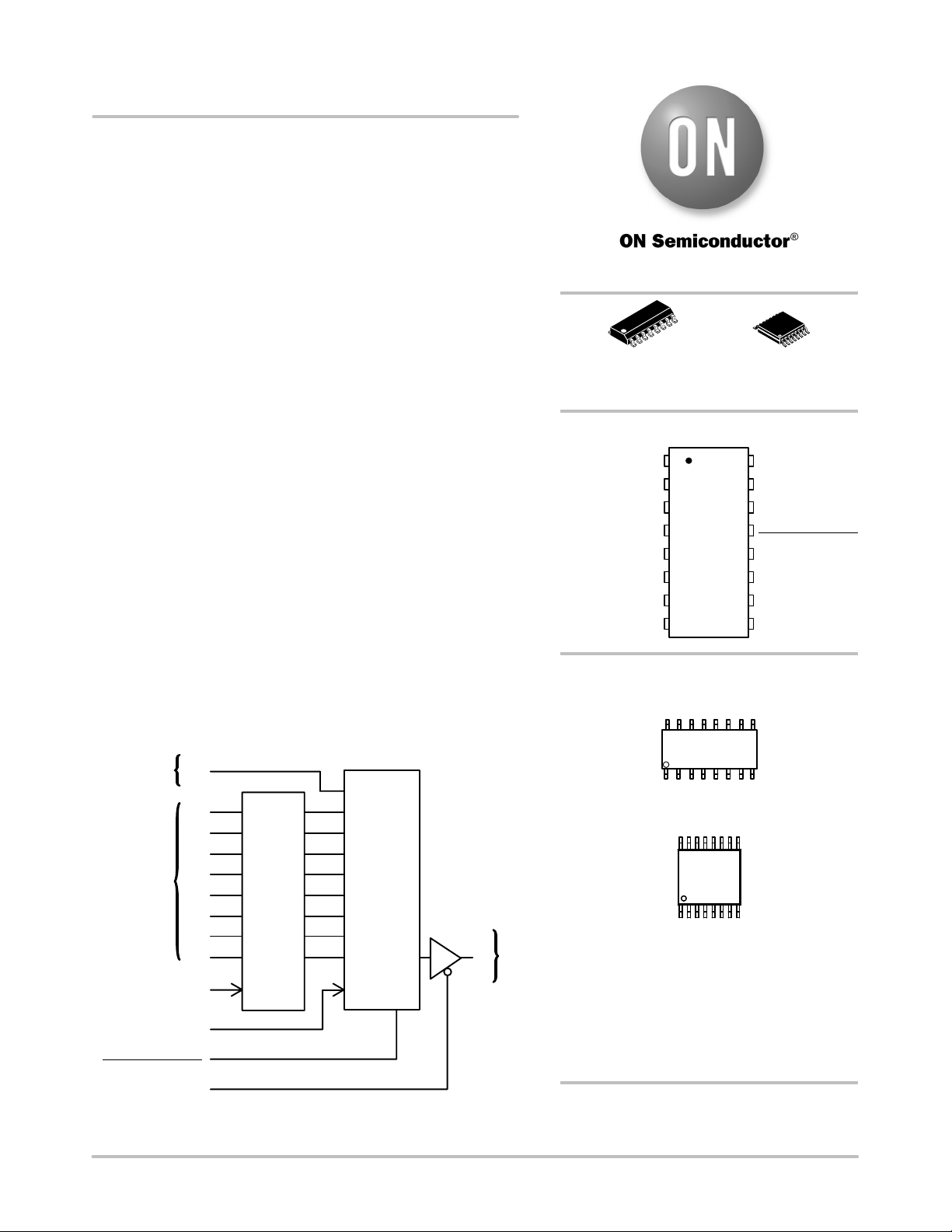
The MC74HC589A device consists of an 8−bit storage latch which
feeds parallel data to an 8−bit shift register. Data can also be loaded
serially (see the Function Table). The shift register output, Q
H
, is a
3−state output, allowing this device to be used in bus−oriented
systems.
The HC589A directly interfaces with the SPI serial data port on
CMOS MPUs and MCUs.
Features
• Output Drive Capability: 15 LSTTL Loads
• Outputs Directly Interface to CMOS, NMOS, and TTL
• Operating Voltage Range: 2.0 to 6.0 V
• Low Input Current: 1 mA
• High Noise Immunity Characteristic of CMOS Devices
• In Compliance with the Requirements Defined by JEDEC
Standard No. 7 A
• Chip Complexity: 526 FETs or 131.5 Equivalent Gates
• NLV Prefix for Automotive and Other Applications Requiring
Unique Site and Control Change Requirements; AEC−Q100
Qualified and PPAP Capable
• These Devices are Pb−Free, Halogen Free and are RoHS Compliant
Figure 1. Logic Diagram
SERIAL
DATA
INPUT
14
15
1
2
3
4
5
6
7
12
11
13
10
S
A
A
B
C
D
E
F
G
H
LATCH CLOCK
SHIFT CLOCK
SERIAL SHIFT/
PARALLEL LOAD
OUTPUT ENABLE
PARALLEL
DATA
INPUTS
DATA
LATCH
SHIFT
REGISTER
V
CC
= PIN 16
GND = PIN 8
9
Q
H
SERIAL
DATA
OUTPUT
See detailed ordering and shipping information in the package
dimensions section on page 10 of this data sheet.
ORDERING INFORMATION
http://onsemi.com
MARKING DIAGRAMS
SOIC−16
TSSOP−16
1
16
HC589AG
AWLYWW
HC
589A
ALYWG
G
1
16
A = Assembly Location
WL, L = Wafer Lot
YY, Y = Year
WW, W = Work Week
G or G = Pb−Free Package
(Note: Microdot may be in either location)
SOIC−16
D SUFFIX
CASE 751B
TSSOP−16
DT SUFFIX
CASE 948F
PIN ASSIGNMENT
13
14
15
16
9
10
11
125
4
3
2
1
8
7
6
LATCH CLOCK
SERIAL SHIFT/
PARALLEL LOA
D
S
A
A
V
CC
Q
H
OUTPUT
ENABLE
SHIFT CLOCK
E
D
C
B
GND
H
G
F
器件 Datasheet 文档搜索
AiEMA 数据库涵盖高达 72,405,303 个元件的数据手册,每天更新 5,000 多个 PDF 文件
