Datasheet 搜索 > 触发器 > ON Semiconductor(安森美) > MC74HC74ADR2 数据手册 > MC74HC74ADR2 其他数据使用手册 1/9 页

 器件3D模型
¥ 1.293
MC74HC74ADR2 其他数据使用手册 - ON Semiconductor(安森美)
制造商:
ON Semiconductor(安森美)
分类:
触发器
封装:
SOIC-14
描述:
双D触发器具有置位和复位高性能硅栅CMOS Dual D Flip−Flop with Set and Reset High−Performance Silicon−Gate CMOS
Pictures:
3D模型
符号图
焊盘图
引脚图
产品图
页面导航:
引脚图在P1Hot
典型应用电路图在P1P5
封装尺寸在P6P8
焊盘布局在P6P8
型号编码规则在P1P4P9
标记信息在P1P6P8P9
封装信息在P4
技术参数、封装参数在P4
应用领域在P1P4
电气规格在P3
型号编号列表在P2
导航目录
MC74HC74ADR2数据手册
Page:
of 9 Go
若手册格式错乱,请下载阅览PDF原文件
© Semiconductor Components Industries, LLC, 2014
August, 2014 − Rev. 14
1 Publication Order Number:
MC74HC74A/D
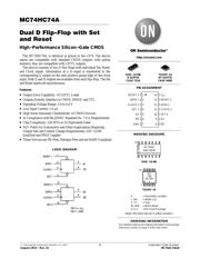
MC74HC74A
Dual D Flip-Flop with Set
and Reset
High−Performance Silicon−Gate CMOS
The MC74HC74A is identical in pinout to the LS74. The device
inputs are compatible with standard CMOS outputs; with pullup
resistors, they are compatible with LSTTL outputs.
This device consists of two D flip−flops with individual Set, Reset,
and Clock inputs. Information at a D−input is transferred to the
corresponding Q output on the next positive going edge of the clock
input. Both Q and Q
outputs are available from each flip−flop. The Set
and Reset inputs are asynchronous.
Features
• Output Drive Capability: 10 LSTTL Loads
• Outputs Directly Interface to CMOS, NMOS, and TTL
• Operating Voltage Range: 2.0 to 6.0 V
• Low Input Current: 1.0 mA
• High Noise Immunity Characteristic of CMOS Devices
• In Compliance with the JEDEC Standard No. 7.0 A Requirements
• Chip Complexity: 128 FETs or 32 Equivalent Gates
• NLV Prefix for Automotive and Other Applications Requiring
Unique Site and Control Change Requirements; AEC−Q100
Qualified and PPAP Capable
• These Devices are Pb−Free, Halogen Free and are RoHS Compliant
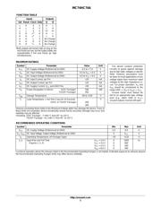
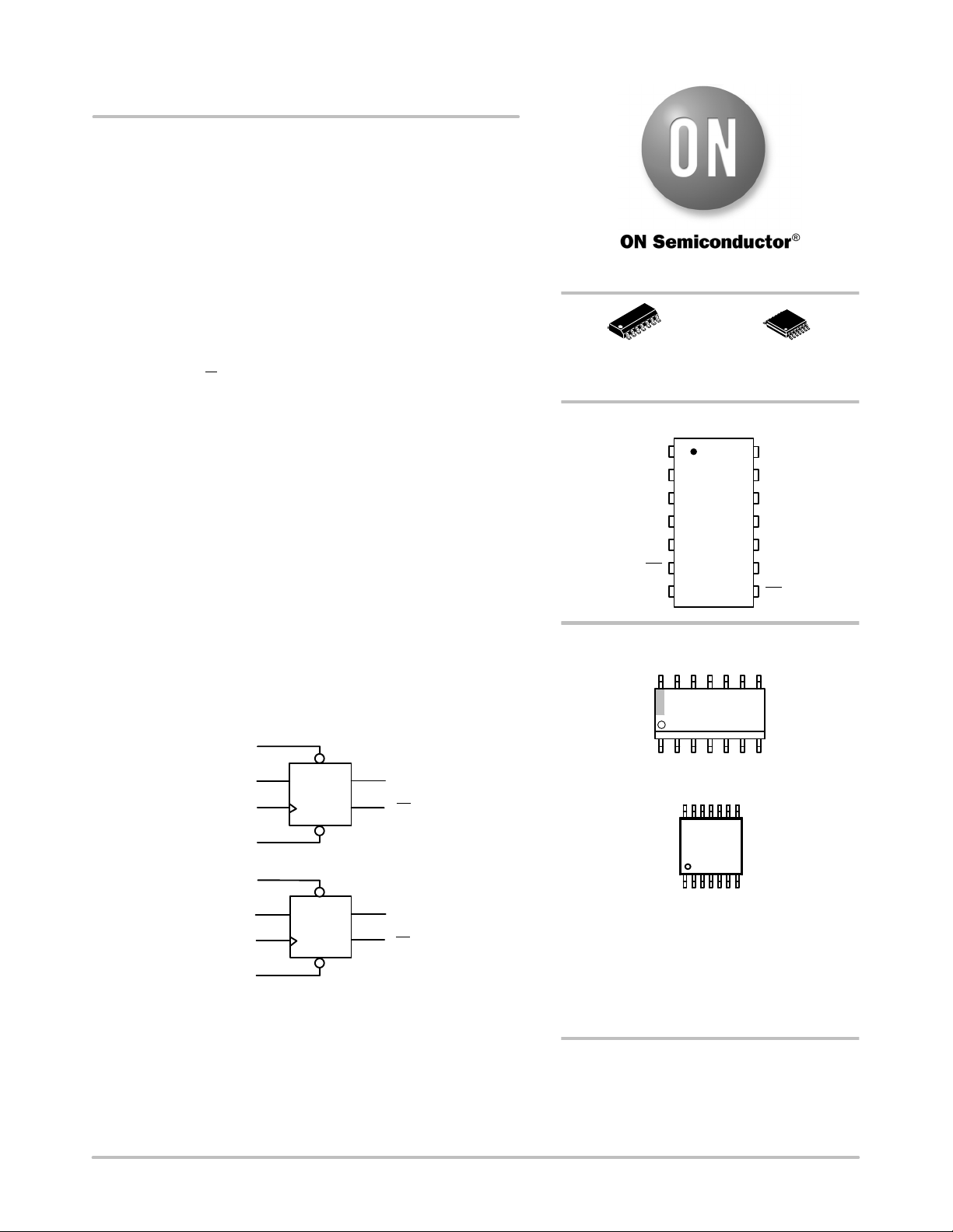
RESET 1
DATA 1
CLOCK 1
SET 1
RESET 2
DATA 2
CLOCK 2
SET 2
1
2
3
4
13
12
11
10
5
6
9
8
Q1
Q1
Q2
Q2
PIN 14 = V
CC
PIN 7 = GND
LOGIC DIAGRAM
http://onsemi.com
See detailed ordering and shipping information in the package
dimensions section on page 4 of this data sheet.
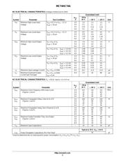
ORDERING INFORMATION
MARKING DIAGRAMS
A = Assembly Location
L, WL = Wafer Lot
Y, YY = Year
W, WW = Work Week
G or G = Pb−Free Package
TSSOP−14
DT SUFFIX
CASE 948G
SOIC−14 NB
D SUFFIX
CASE 751A
HC74AG
AWLYWW
1
14
HC
74A
ALYWG
G
1
14
(Note: Microdot may be in either location)
TSSOP−14
SOIC−14 NB
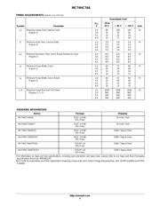
PIN ASSIGNMENT
SET 1
CLOCK 1
DATA 1
RESET 1
11
12
13
14
8
9
105
4
3
2
1
7
6
SET 2
CLOCK 2
DATA 2
RESET 2
V
CC
Q2
Q2
GND
Q1
Q1
器件 Datasheet 文档搜索
AiEMA 数据库涵盖高达 72,405,303 个元件的数据手册,每天更新 5,000 多个 PDF 文件
