Datasheet 搜索 > 逻辑控制器 > ON Semiconductor(安森美) > MC74LCX125DT 数据手册 > MC74LCX125DT 其他数据使用手册 1/9 页

 器件3D模型
¥ 0.864
MC74LCX125DT 其他数据使用手册 - ON Semiconductor(安森美)
制造商:
ON Semiconductor(安森美)
分类:
逻辑控制器
封装:
TSSOP-14
描述:
低电压CMOS四路缓冲电压为5 V容限输入和输出(三态,非反相) Low-Voltage CMOS Quad Buffer With 5 V−Tolerant Inputs and Outputs (3−State, Non−Inverting)
Pictures:
3D模型
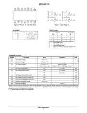
符号图
焊盘图
引脚图
产品图
页面导航:
导航目录
MC74LCX125DT数据手册
Page:
of 9 Go
若手册格式错乱,请下载阅览PDF原文件
Semiconductor Components Industries, LLC, 2012
October, 2012 − Rev. 8
1 Publication Order Number:
MC74LCX125/D
MC74LCX125
Low-Voltage CMOS
Quad Buffer
With 5 V−Tolerant Inputs and Outputs
(3−State, Non−Inverting)
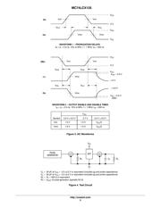
The MC74LCX125 is a high performance, non−inverting quad
buffer operating from a 2.3 to 3.6 V supply. High impedance TTL
compatible inputs significantly reduce current loading to input drivers
while TTL compatible outputs offer improved switching noise
performance. A V
I
specification of 5.5 V allows MC74LCX125 inputs
to be safely driven from 5.0 V devices. The MC74LCX125 is suitable
for memory address driving and all TTL level bus oriented transceiver
applications.
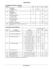
Current drive capability is 24 mA at the outputs. The Output Enable
(OE
n) inputs, when HIGH, disable the outputs by placing them in a
HIGH Z condition.
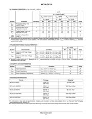
Features
Designed for 2.3 to 3.6 V V
CC
Operation
5.0 V Tolerant − Interface Capability With 5.0 V TTL Logic
Supports Live Insertion and Withdrawal
I
OFF
Specification Guarantees High Impedance When V
CC
= 0 V
LVTTL Compatible
LVCMOS Compatible
24 mA Balanced Output Sink and Source Capability
Near Zero Static Supply Current in all Three Logic States (10 mA)
Substantially Reduces System Power Requirements
Latchup Performance Exceeds 500 mA
ESD Performance: Human Body Model >2000 V
Machine Model >200 V
NLV Prefix for Automotive and Other Applications Requiring
Unique Site and Control Change Requirements; AEC−Q100
Qualified and PPAP Capable
These Devices are Pb−Free, Halogen Free/BFR Free and are RoHS
Compliant
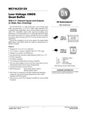
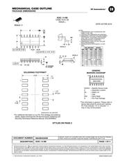
MARKING
DIAGRAMS
TSSOP−14
DT SUFFIX
CASE 948G
14
1
SOIC−14
D SUFFIX
CASE 751A
14
1
See detailed ordering and shipping information in the package
dimensions section on page 4 of this data sheet.
ORDERING INFORMATION
http://onsemi.com
LCX125G
AWLYWW
1
14
LCX
125
ALYWG
G
1
14
A = Assembly Location
L, WL = Wafer Lot
Y, YY = Year
W, WW = Work Week
G or G = Pb−Free Package
(Note: Microdot may be in either location)
器件 Datasheet 文档搜索
AiEMA 数据库涵盖高达 72,405,303 个元件的数据手册,每天更新 5,000 多个 PDF 文件
