Datasheet 搜索 > 逻辑芯片 > ON Semiconductor(安森美) > MC74VHC1G14DFT1 数据手册 > MC74VHC1G14DFT1 其他数据使用手册 1/15 页

¥ 0.359
MC74VHC1G14DFT1 其他数据使用手册 - ON Semiconductor(安森美)
制造商:
ON Semiconductor(安森美)
分类:
逻辑芯片
封装:
SC-70
描述:
施密特触发器逆变器 Schmitt-Trigger Inverter
Pictures:
3D模型
符号图
焊盘图
引脚图
产品图
页面导航:
引脚图在P2Hot
封装尺寸在P8P9P10P11P12P13P14P15
焊盘布局在P9P10P11P12P15
型号编码规则在P1P7P15
标记信息在P1P15
封装信息在P7
技术参数、封装参数在P7
应用领域在P1P7
电气规格在P4P5
型号编号列表在P3
导航目录
MC74VHC1G14DFT1数据手册
Page:
of 15 Go
若手册格式错乱,请下载阅览PDF原文件
© Semiconductor Components Industries, LLC, 2013
June, 2021 − Rev. 24
1 Publication Order Number:
MC74VHC1G14/D
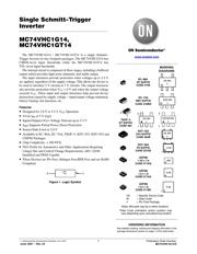
Single Schmitt-Trigger
Inverter
MC74VHC1G14,
MC74VHC1GT14
The MC74VHC1G14 / MC74VHC1GT14 is a single Schmitt−
Trigger Inverter in tiny footprint packages. The MC74VHC1G14 has
CMOS−level input thresholds while the MC74VHC1GT14 has
TTL−level input thresholds.
The internal circuit is composed of three stages, including a buffered
output which provides high noise immunity and stable output.
The input structures provide protection when voltages up to 5.5 V
are applied, regardless of the supply voltage. This allows the device to
be used to interface 5 V circuits to 3 V circuits. The output structures
also provide protection when V
CC
= 0 V and when the output voltage
exceeds V
CC
. These input and output structures help prevent device
destruction caused by supply voltage − input/output voltage mismatch,
battery backup, hot insertion, etc.
Features
• Designed for 2.0 V to 5.5 V V
CC
Operation
• 4.0 ns t
PD
at 5 V (typ)
• Inputs/Outputs Over−Voltage Tolerant up to 5.5 V
• I
OFF
Supports Partial Power Down Protection
• Source/Sink 8 mA at 3.0 V
• Available in SC−88A, SC−74A, TSOP−5, SOT−553, SOT−953 and
UDFN6 Packages
• Chip Complexity < 100 FETs
• NLV Prefix for Automotive and Other Applications Requiring
Unique Site and Control Change Requirements; AEC−Q100
Qualified and PPAP Capable
• These Devices are Pb−Free, Halogen Free/BFR Free and are RoHS
Compliant
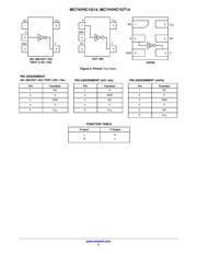
Figure 1. Logic Symbol
A
Y
1
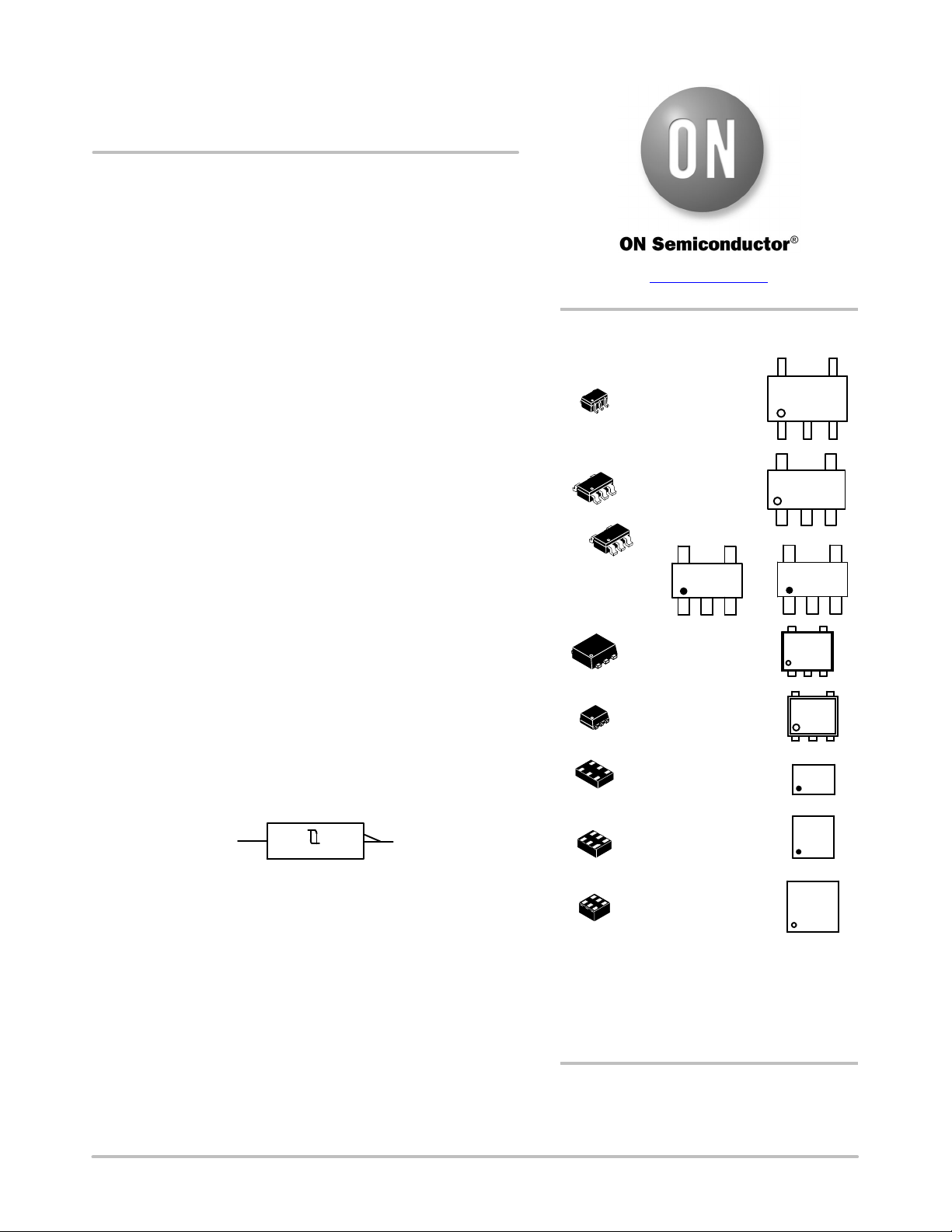
See detailed ordering, marking and shipping information in the
package dimensions section on page 7 of this data sheet.
ORDERING INFORMATION
www.onsemi.com
SC−88A
DF SUFFIX
CASE 419A
SOT−553
XV5 SUFFIX
CASE 463B
XX MG
G
XX = Specific Device Code
M = Date Code*
G = Pb−Free Package
XX MG
G
(Note: Microdot may be in either location)
*Date Code orientation and/or position may
vary depending upon manufacturing location.
UDFN6
1.0 x 1.0
CASE 517BX
X M
1
SOT−953
P5 SUFFIX
CASE 527AE
X M
1
XXX MG
G
SC−74A
DBV SUFFIX
CASE 318BQ
XM
UDFN6
1.45 x 1.0
CASE 517AQ
MARKING
DIAGRAMS
UDFN6
1.2 x 1.0
CASE 517AA
X M
1
5
XX MG
G
TSOP−5
DT SUFFIX
CASE 483
1
5
1
5
XXXAYWG
G
器件 Datasheet 文档搜索
AiEMA 数据库涵盖高达 72,405,303 个元件的数据手册,每天更新 5,000 多个 PDF 文件
