Datasheet 搜索 > 稳压芯片 > ON Semiconductor(安森美) > MC78M05CDTRK 数据手册 > MC78M05CDTRK 产品描述及参数 1/15 页
 器件3D模型
¥ 1.578
MC78M05CDTRK 产品描述及参数 - ON Semiconductor(安森美)
制造商:
ON Semiconductor(安森美)
分类:
稳压芯片
封装:
TO-252-3
描述:
三端中电流正固定电压稳压器
Pictures:
3D模型
符号图
焊盘图
引脚图
产品图
页面导航:
原理图在P1
封装尺寸在P14P15
焊盘布局在P14
型号编码规则在P1P10P11P12P13P15
标记信息在P1P10P11P12P13P15
封装信息在P10P11P12P13
技术参数、封装参数在P10P11P12P13
应用领域在P1P9P10P11P12P13
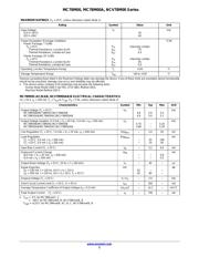
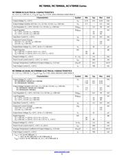
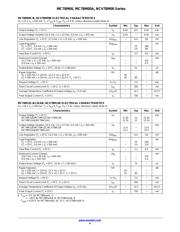
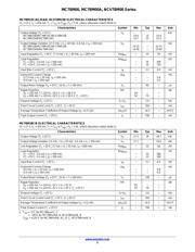
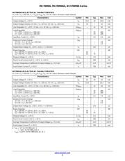
电气规格在P2P3P4P5P6
型号编号列表在P2
导航目录
MC78M05CDTRK数据手册
Page:
of 15 Go
若手册格式错乱,请下载阅览PDF原文件
© Semiconductor Components Industries, LLC, 2016
March, 2016 − Rev. 28
1 Publication Order Number:
MC78M00/D
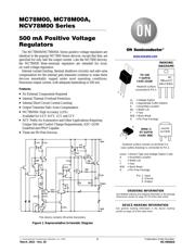
MC78M00, MC78M00A,
NCV78M00 Series
500 mA Positive Voltage
Regulators
The MC78M00/MC78M00A Series positive voltage regulators are
identical to the popular MC7800 Series devices, except that they are
specified for only half the output current. Like the MC7800 devices,
the MC78M00 three−terminal regulators are intended for local,
on−card voltage regulation.
Internal current limiting, thermal shutdown circuitry and safe−area
compensation for the internal pass transistor combine to make these
devices remarkably rugged under most operating conditions.
Maximum output current, with adequate heatsinking is 500 mA.
Features
• No External Components Required
• Internal Thermal Overload Protection
• Internal Short Circuit Current Limiting
• Output Transistor Safe−Area Compensation
• MC78M00A High Accuracy (±2%)
Available for 5.0 V, 8.0 V, 12 V and 15 V
• NCV Prefix for Automotive and Other Applications Requiring
Unique Site and Control Change Requirements; AEC−Q100
Qualified and PPAP Capable
• These are Pb−Free Devices
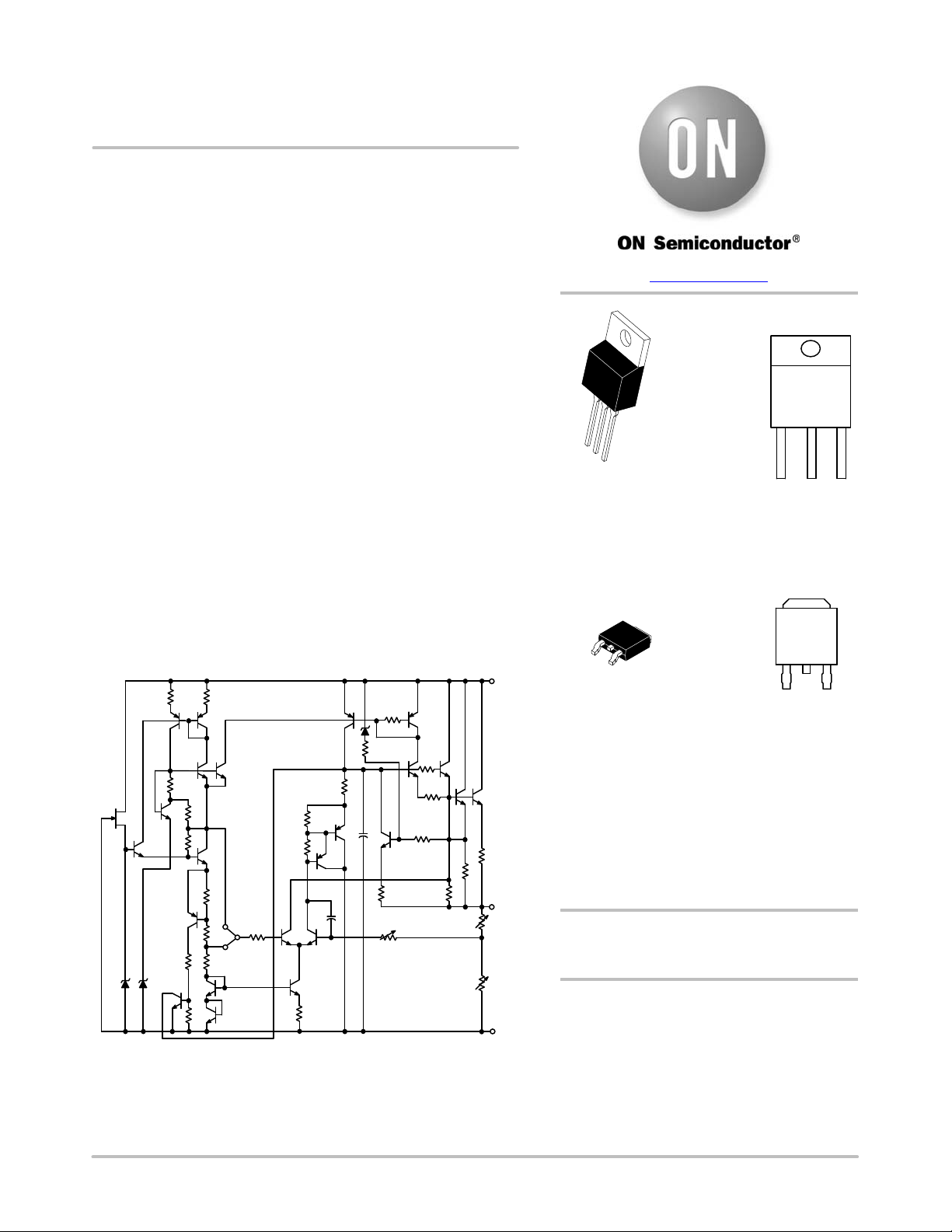
Figure 1. Representative Schematic Diagram
This device contains 28 active transistors.
1.0 k 1.0 k
Input
210
6.7
V
16 k
100
200
300
3.6
k
6.4
k
520
6.0 k
2.0 k 3.9 k
6.0
k
2.8 k
40
pF
5.6 k
3.0 k
1.0 k
300
20050
13
0.24
GND
Output
10 pF
2.6 k
TO−220
T SUFFIX
CASE 221AB
1
DPAK−3
DT SUFFIX
CASE 369C
MARKING
DIAGRAMS
xxxxx = Device Type and Voltage Option Code
A = Assembly Location
L = Wafer Lot
Y = Year
WW = Work Week
G = Pb−Free Package
2
3
See detailed ordering and shipping information in the packag
e
dimensions section on page 10−14 of this data sheet.
ORDERING INFORMATION
Heatsink surface
connected to Pin 2.
Pin 1. Input
2. Ground
3. Output
Heatsink surface (shown as terminal 4 in
case outline drawing) is connected to Pin 2.
MC
AWLYWWG
78MxxXXT
www.onsemi.com
1
2
3
4
xxxxxG
ALYWW
xx = Voltage Option
XX = Appropriate Suffix Options
A = Assembly Location
WL = Wafer Lot
Y = Year
WW = Work Week
G = Pb−Free Package
See general marking information in the device marking
section on page 10 of this data sheet.
DEVICE MARKING INFORMATION
器件 Datasheet 文档搜索
AiEMA 数据库涵盖高达 72,405,303 个元件的数据手册,每天更新 5,000 多个 PDF 文件
