Datasheet 搜索 > 8位微控制器 > NXP(恩智浦) > MC9S08AW16CFGER 数据手册 > MC9S08AW16CFGER 其他数据使用手册 1/37 页
 器件3D模型
¥ 46.724
MC9S08AW16CFGER 其他数据使用手册 - NXP(恩智浦)
制造商:
NXP(恩智浦)
分类:
8位微控制器
封装:
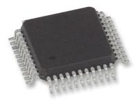
LQFP-44
描述:
NXP MC9S08AW16CFGER 微控制器, 8位, 通用 AW系列, S08AW, 40 MHz, 16 KB, 1 KB, 44 引脚, LQFP
Pictures:
3D模型
符号图
焊盘图
引脚图
产品图
页面导航:
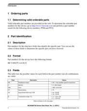
引脚图在P30P31P33Hot
封装尺寸在P29
技术参数、封装参数在P1P6P14P15P16
型号编号列表在P4
导航目录
MC9S08AW16CFGER数据手册
Page:
of 37 Go
若手册格式错乱,请下载阅览PDF原文件

MC9S08PT60
MC9S08PT60 Series
Support: MC9S08PT60 and
MC9S08PT32
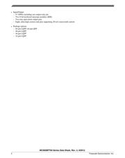
Features
•
8-Bit S08 central processor unit (CPU)
– Up to 20 MHz bus at 2.7 V to 5.5 V across
temperature range of -40 °C to 105 °C
– Supporting up to 40 interrupt/reset sources
– Supporting up to four-level nested interrupt
– On-chip memory
– Up to 60 KB flash read/program/erase over full
operating voltage and temperature
– Up to 256 byte EEPROM; 2-byte erase sector;
program and erase while executing flash
– Up to 4096 byte random-access memory (RAM)
– Flash and RAM access protection
•
Power-saving modes
– One low-power stop mode; reduced power wait
mode
– Peripheral clock enable register can disable clocks to
unused modules, reducing currents; allows clocks to
remain enabled to specific peripherals in stop3 mode
•
Clocks
– Oscillator (XOSC) - loop-controlled Pierce
oscillator; crystal or ceramic resonator range of
31.25 kHz to 39.0625 kHz or 4 MHz to 20 MHz
– Internal clock source (ICS) - containing a frequency-
locked-loop (FLL) controlled by internal or external
reference; precision trimming of internal reference
allowing 1% deviation across temperature range of 0
°C to 70 °C and 2% deviation across temperature
range of -40 °C to 105 °C; up to 20 MHz
•
System protection
– Watchdog with independent clock source
– Low-voltage detection with reset or interrupt;
selectable trip points
– Illegal opcode detection with reset
– Illegal address detection with reset
•
Development support
– Single-wire background debug interface
– Breakpoint capability to allow three breakpoints
setting during in-circuit debugging
– On-chip in-circuit emulator (ICE) debug module
containing two comparators and nine trigger modes
•
Peripherals
– ACMP - one analog comparator with both positive
and negative inputs; separately selectable interrupt
on rising and falling comparator output; filtering
– ADC - 16-channel, 12-bit resolution; 2.5 µs
conversion time; data buffers with optional
watermark; automatic compare function; internal
bandgap reference channel; operation in stop mode;
optional hardware trigger
– CRC - programmable cyclic redundancy check
module
– FTM - three flex timer modulators modules
including one 6-channel and two 2-channel ones;
16-bit counter; each channel can be configured for
input capture, output compare, edge- or center-
aligned PWM mode
– IIC - One inter-integrated circuit module; up to 400
kbps; multi-master operation; programmable slave
address; supporting broadcast mode and 10-bit
addressing
– MTIM - Two modulo timers with 8-bit prescaler and
overflow interrupt
– RTC - 16-bit real timer counter (RTC)
– SCI - three serial communication interface (SCI/
UART) modules optional 13-bit break; full duplex
non-return to zero (NRZ); LIN extension support
– SPI - one 8-bit and one 16-bit serial peripheral
interface (SPI) modules; full-duplex or single-wire
bidirectional; master or slave mode
– TSI - supporting up to 16 external electrodes;
configurable software or hardware scan trigger; fully
support freescale touch sensing software library;
capability to wake MCU from stop3 mode
Freescale Semiconductor
Document Number: MC9S08PT60
Data Sheet: Technical Data
Rev. 3, 4/2012
Freescale reserves the right to change the detail specifications as may be
required to permit improvements in the design of its products.
© 2011–2012 Freescale Semiconductor, Inc.
器件 Datasheet 文档搜索
AiEMA 数据库涵盖高达 72,405,303 个元件的数据手册,每天更新 5,000 多个 PDF 文件
