Datasheet 搜索 > 8位微控制器 > NXP(恩智浦) > MC9S08QD4CSCR 数据手册 > MC9S08QD4CSCR 产品描述及参数 1/53 页
 器件3D模型
¥ 13.225
MC9S08QD4CSCR 产品描述及参数 - NXP(恩智浦)
制造商:
NXP(恩智浦)
分类:
8位微控制器
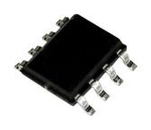
封装:
SOIC-8
描述:
8位 MCU微控制单元, HCS08 Family S08QD Series Microcontrollers, 16 MHz, 4 KB, 256 Byte, 8 引脚, SOIC
Pictures:
3D模型
符号图
焊盘图
引脚图
产品图
页面导航:
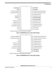
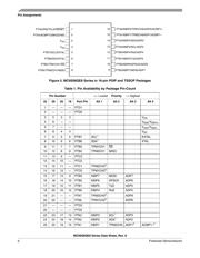
引脚图在P4P5P6P7Hot
原理图在P3
封装尺寸在P31
型号编码规则在P30
技术参数、封装参数在P1P8P17P18P19P24P25P29
电气规格在P7P8P9P10P11P12P13P14P15P16P17P18

导航目录
MC9S08QD4CSCR数据手册
Page:
of 53 Go
若手册格式错乱,请下载阅览PDF原文件

Freescale Semiconductor
Data Sheet: Technical Data
An Energy Efficient Solution by Freescale
Document Number: MC9S08QE8
Rev. 8, 4/2011
© Freescale Semiconductor, Inc., 2007-2011. All rights reserved.
This document contains information on a product under development. Freescale reserves the
right to change or discontinue this product without notice.
MC9S08QE8
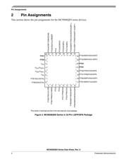
32-Pin LQFP
Case 873A
28-Pin SOIC
751F-05
16-Pin PDIP
648
16-Pin TSSOP
948F
20-Pin SOIC
751D-07
32-Pin QFN
Case 2078-01
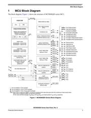
Features
• 8-Bit HCS08 Central Processor Unit (CPU)
– Up to 20 MHz CPU at 3.6 V to 1.8 V across temperature range of
–40 °C to 85 °C
– HC08 instruction set with added BGND instruction
– Support for up to 32 interrupt/reset sources
•On-Chip Memory
– Flash read/program/erase over full operating voltage and
temperature
– Random-access memory (RAM)
– Security circuitry to prevent unauthorized access to RAM and
flash contents
• Power-Saving Modes
– Two low power stop modes
– Reduced power wait mode
– Low power run and wait modes allow peripherals to run while
voltage regulator is in standby
– Peripheral clock gating register can disable clocks to unused
modules, thereby reducing currents
– Very low power external oscillator that can be used in stop2 or
stop3 modes to provide accurate clock source to real time counter
–6 s typical wake-up time from stop3 mode
• Clock Source Options
– Oscillator (XOSC) — Loop-control Pierce oscillator; crystal or
ceramic resonator range of 31.25 kHz to 38.4 kHz or 1 MHz to
16 MHz
– Internal Clock Source (ICS) — Internal clock source module
containing a frequency-locked-loop (FLL) controlled by internal
or external reference; precision trimming of internal reference
allows 0.2% resolution and 2% deviation over temperature and
voltage; supporting bus frequencies from 1 MHz to 10 MHz
• System Protection
– Watchdog computer operating properly (COP) reset with option to
run from dedicated 1 kHz internal clock source or bus clock
– Low-voltage warning with interrupt
– Low-voltage detection with reset or interrupt
– Illegal opcode detection with reset
– Illegal address detection with reset
– Flash block protection
• Development Support
– Single-wire background debug interface
– Breakpoint capability to allow single breakpoint setting during
in-circuit debugging (plus two more breakpoints in on-chip debug
module)
– On-chip in-circuit emulator (ICE) debug module containing two
comparators and nine trigger modes; eight deep FIFO for storing
change-of-flow addresses and event-only data; debug module
supports both tag and force breakpoints
• Peripherals
– ADC — 10-channel, 12-bit resolution; 2.5 s conversion time;
automatic compare function; 1.7 mV/C temperature sensor;
internal bandgap reference channel; operation in stop3; fully
functional from 3.6 V to 1.8 V
– ACMPx — Two analog comparators with selectable interrupt on
rising, falling, or either edge of comparator output; compare
option to fixed internal bandgap reference voltage; outputs can be
optionally routed to TPM module; operation in stop3
– SCI — Full-duplex non-return to zero (NRZ); LIN master
extended break generation; LIN slave extended break detection;
wake-up on active edge
– SPI — Full-duplex or single-wire bidirectional; double-buffered
transmit and receive; master or slave mode; MSB-first or
LSB-first shifting
– IIC — Up to 100 kbps with maximum bus loading; multi-master
operation; programmable slave address; interrupt driven
byte-by-byte data transfer; supporting broadcast mode and 10-bit
addressing
– TPMx — Two 3-channel (TPM1 and TPM2); selectable input
capture, output compare, or buffered edge- or center-aligned
PWM on each channel
– RTC — (Real-time counter) 8-bit modulus counter with binary or
decimal based prescaler; external clock source for precise time
base, time-of-day, calendar or task scheduling functions; free
running on-chip low power oscillator (1 kHz) for cyclic wakeup
without external components; runs in all MCU modes
• Input/Output
– 26 GPIOs, one output-only pin and one input-only pin
– Eight KBI interrupts with selectable polarity
– Hysteresis and configurable pullup device on all input pins;
configurable slew rate and drive strength on all output pins.
• Package Options
– 32-pin LQFP, 32-pin QFN, 28-pin SOIC, 20-pin SOIC,
16-pin PDIP, 16-pin TSSOP
Document Number: MC9S08QE8
Rev. 8, 4/2011
MC9S08QE8 Series
Covers: MC9S08QE8 and
MC9S08QE4
器件 Datasheet 文档搜索
AiEMA 数据库涵盖高达 72,405,303 个元件的数据手册,每天更新 5,000 多个 PDF 文件
