Datasheet 搜索 > NXP(恩智浦) > MC9S12A64CFU 数据手册 > MC9S12A64CFU 其他数据使用手册 1/2 页

 器件3D模型
¥ 37.768
MC9S12A64CFU 其他数据使用手册 - NXP(恩智浦)
制造商:
NXP(恩智浦)
封装:
QFP
Pictures:
3D模型
符号图
焊盘图
引脚图
产品图
页面导航:
应用领域在P1
导航目录
MC9S12A64CFU数据手册
Page:
of 2 Go
若手册格式错乱,请下载阅览PDF原文件

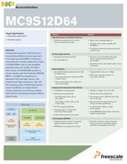
2 x SCI
1 x SPI
1 x CAN
2.0 A/B
PWM
8-bit, 8 ch./16-bit, 4 ch.
Internal Bus
HCS12 CPU
16-Key Wake-Up
IRQ Ports
Vreg
5V to 2.5V
Enhanced Capture Timer
16-bit, 8-ch.
ATD0
10-bit, 8-ch.
4 KB RAM
64 KB Flash
1 KB EEPROM
I
2
C
ATD1
10-bit, 8-ch.
16-bit Microcontrollers
MC9S12D64
Overview
Freescale Semiconductor’s HCS12 Family of
microcontrollers (MCUs) is the next generation
of the highly successful 68HC12 architecture.
Using Freescale’s industry-leading 0.25 µs Flash,
the MC9S12D64 is part of a pin-compatible
family that scales from 32 KB to 512 KB of
Flash memory. The MC9S12D64 provides an
upward migration path from Freescale’s 68HC08,
68HC11 and 68HC12 architectures for
applications that need larger memory, more
peripherals and higher performance. Also, with
the increasing number of CAN-based electronic
control units (ECUs), its multiple network
modules support this environment by enabling
highly efficient communications between different
network buses.
Target Applications
>
Automotive applications
>
Industrial control
Features Benefits
H
igh-Performance 16-bit HCS12 CPU Core
On-Chip Debug Interface
> Dedicated serial debug interface
> On-chip breakpoints
> Real-time in-circuit emulation and debug
without expensive and cumbersome
box emulators
> Read/write memory and registers while running
at full speed
N
etwork Modules
> One msCAN module implementing the CAN
2.0 A/B protocol
• Five receive buffers per module with FIFO
storage scheme
• Three transmit buffers per module with
internal prioritization
> Programmable bit rate up to 1 Mbps
> FIFO receive approach superior for
event-driven networks
Integrated Third-Generation Flash Memory
1 KB Integrated EEPROM
> Flexible protection scheme for protection
against accidental program or erase
> EEPROM can be programmed in 46 µs
> Can erase 4 bytes at a time and program
2 bytes at a time for calibration, security,
personality and diagnostic information
> 25 MHz bus operation at 5V for 40 ns
minimum instruction cycle time
> Object code compatible 68HC12
> Assembly source code compatible with
the 68HC11
> C-optimized architecture produces extremely
compact code
> In-application reprogrammable
> Self-timed, fast programming
• Fast Flash page erase—20 ms
(512 bytes)
• Can program 16 bits in 20 µs while
in burst mode
>
5V Flash program/erase/read
>
Flash granularity—512 byte Flash
erase/2 byte Flash program
> Flexible block protection and security
> Flexibility to change code in the field
> Efficient end-of-line programming
> Total program time for 256 KB code is less
than 10 seconds
> Reduces production programming cost
through ultra-fast programming
>
No external high voltage or charge
pump required
>
Virtual EEPROM implementation, Flash array
usable for EE extension
器件 Datasheet 文档搜索
AiEMA 数据库涵盖高达 72,405,303 个元件的数据手册,每天更新 5,000 多个 PDF 文件
