Datasheet 搜索 > 16位微控制器 > NXP(恩智浦) > MC9S12E128CFUE 数据手册 > MC9S12E128CFUE 产品描述及参数 1/51 页
 器件3D模型
¥ 139.173
MC9S12E128CFUE 产品描述及参数 - NXP(恩智浦)
制造商:
NXP(恩智浦)
分类:
16位微控制器
封装:
QFP-80
描述:
NXP MC9S12E128CFUE 微控制器, 16位, S12E, 25 MHz, 128 KB, 8 KB, 80 引脚, QFP
Pictures:
3D模型
符号图
焊盘图
引脚图
产品图
页面导航:
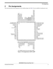
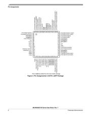
引脚图在P5P6P7P8P9P10P11Hot
原理图在P3
封装尺寸在P34P35P36P37P38P39P40P41P42P43P44P45
型号编码规则在P34
技术参数、封装参数在P1P12P21P22P23P30P33
电气规格在P12P13P14P15P16P17P18P19P20P21P22P23
导航目录
MC9S12E128CFUE数据手册
Page:
of 51 Go
若手册格式错乱,请下载阅览PDF原文件
Freescale Semiconductor
Data Sheet: Technical Data
Document Number: MC9S08QE128
Rev. 7, 10/2008
© Freescale Semiconductor, Inc., 2008. All rights reserved.
Freescale reserves the right to change the detail specifications as may be required to permit
improvements in the design of its products.
MC9S08QE128
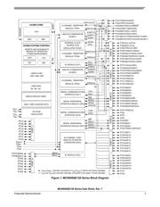
• 8-Bit HCS08 Central Processor Unit (CPU)
– Up to 50.33-MHz HCS08 CPU above 2.4V, 40-MHz
CPU above 2.1V, and 20-MHz CPU above 1.8V, across
temperature range
– HC08 instruction set with added BGND instruction
– Support for up to 32 interrupt/reset sources
•On-Chip Memory
– Flash read/program/erase over full operating voltage
and temperature
– Random-access memory (RAM)
– Security circuitry to prevent unauthorized access to
RAM and flash contents
• Power-Saving Modes
– Two low power stop modes; reduced power wait mode
– Peripheral clock enable register can disable clocks to
unused modules, reducing currents; allows clocks to
remain enabled to specific peripherals in stop3 mode
– Very low power external oscillator can be used in stop3
mode to provide accurate clock to active peripherals
– Very low power real time counter for use in run, wait,
and stop modes with internal and external clock sources
–6 μs typical wake up time from stop modes
• Clock Source Options
– Oscillator (XOSC) — Loop-control Pierce oscillator;
Crystal or ceramic resonator range of 31.25 kHz to
38.4 kHz or 1 MHz to 16 MHz
– Internal Clock Source (ICS) — FLL controlled by
internal or external reference; precision trimming of
internal reference allows 0.2% resolution and 2%
deviation; supports CPU freq. from 2 to 50.33 MHz
• System Protection
– Watchdog computer operating properly (COP) reset
with option to run from dedicated 1-kHz internal clock
source or bus clock
– Low-voltage detection with reset or interrupt; selectable
trip points
– Illegal opcode detection with reset
– Flash block protection
• Development Support
– Single-wire background debug interface
– Breakpoint capability to allow single breakpoint setting
during in-circuit debugging (plus two more breakpoints)
– On-chip in-circuit emulator (ICE) debug module
containing two comparators and nine trigger modes.
Eight deep FIFO for storing change-of-flow addresses
and event-only data. Debug module supports both tag
and force breakpoints.
• ADC — 24-channel, 12-bit resolution; 2.5 μs conversion
time; automatic compare function; 1.7 mV/°C temperature
sensor; internal bandgap reference channel; operation in
stop3; fully functional from 3.6V to 1.8V
• ACMPx — Two analog comparators with selectable
interrupt on rising, falling, or either edge of comparator
output; compare option to fixed internal bandgap reference
voltage; outputs can be optionally routed to TPM module;
operation in stop3
• SCIx — Two SCIs with full duplex non-return to zero
(NRZ); LIN master extended break generation; LIN slave
extended break detection; wake up on active edge
• SPIx— Two serial peripheral interfaces with Full-duplex or
single-wire bidirectional; Double-buffered transmit and
receive; MSB-first or LSB-first shifting
• IICx — Two IICs with; Up to 100 kbps with maximum bus
loading; Multi-master operation; Programmable slave
address; Interrupt driven byte-by-byte data transfer;
supports broadcast mode and 10 bit addressing
• TPMx — One 6-channel and two 3-channel; Selectable
input capture, output compare, or buffered edge- or
center-aligned PWMs on each channel
• RTC — 8-bit modulus counter with binary or decimal
based prescaler; External clock source for precise time
base, time-of-day, calendar or task scheduling functions;
Free running on-chip low power oscillator (1 kHz) for
cyclic wake-up without external components
• Input/Output
– 70 GPIOs and 1 input-only and 1 output-only pin
– 16 KBI interrupts with selectable polarity
– Hysteresis and configurable pull-up device on all input
pins; Configurable slew rate and drive strength on all
output pins.
– SET/CLR registers on 16 pins (PTC and PTE)
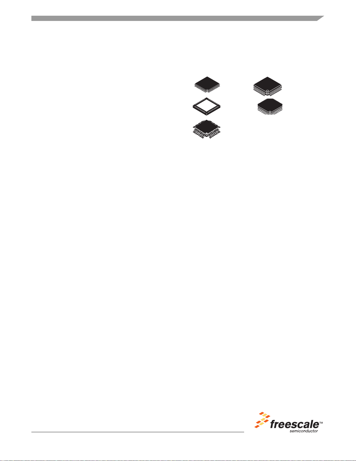
80-LQFP
Case 917A
14 mm
2
64-LQFP
Case 840F
10 mm
2
48-QFN
Case 1314
7 mm
2
32-LQFP
Case 873A
7 mm
2
44-LQFP
Case 824D
10 mm
2
MC9S08QE128 Series
Covers: MC9S08QE128, MC9S08QE96, MC9S08QE64
An Energy Efficient Solution by Freescale
器件 Datasheet 文档搜索
AiEMA 数据库涵盖高达 72,405,303 个元件的数据手册,每天更新 5,000 多个 PDF 文件
