Datasheet 搜索 > 接口芯片 > Microchip(微芯) > MCP2003A-E/MD 数据手册 > MCP2003A-E/MD 其他数据使用手册 3/34 页
 器件3D模型
¥ 6.466
MCP2003A-E/MD 其他数据使用手册 - Microchip(微芯)
制造商:
Microchip(微芯)
分类:
接口芯片
封装:
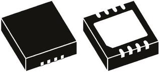
DFN-8
描述:
MCP2003/2004 LIN 收发器### LIN 通信 - Microchip
Pictures:
3D模型
符号图
焊盘图
引脚图
产品图
页面导航:
引脚图在P9Hot
典型应用电路图在P7
原理图在P2
标记信息在P20
封装信息在P20P21P22P23P25P26P31
技术参数、封装参数在P1P4P11P13P14P15P16P18
应用领域在P7
电气规格在P13P14P15
导航目录
MCP2003A-E/MD数据手册
Page:
of 34 Go
若手册格式错乱,请下载阅览PDF原文件
2010-2014 Microchip Technology Inc. DS20002230F-page 3
MCP2003/4/3A/4A
1.0 DEVICE OVERVIEW
The MCP2003/4/3A/4A devices provide a physical
interface between a microcontroller and a LIN bus.
These devices will translate the CMOS/TTL logic levels
to LIN logic level, and vice versa. It is intended for
automotive and industrial applications with serial bus
speeds up to 20 kbaud.
LIN Bus Specification Revision 2.1 requires that the
transceiver of all nodes in the system is connected via
the LIN pin, referenced to ground and with a maximum
external termination resistance load of 510 from LIN
bus to battery supply. The 510 corresponds to
1 master and 15 slave nodes.
The V
REN pin can be used to drive the logic input of an
external voltage regulator. This pin is high in all modes
except for Power-Down mode.
1.1 External Protection
1.1.1 REVERSE BATTERY PROTECTION
An external reverse-battery-blocking diode should be
used to provide polarity protection (see Example 1-1).
1.1.2 TRANSIENT VOLTAGE
PROTECTION (LOAD DUMP)
An external 43V transient suppressor (TVS) diode,
between V
BB and ground, with a 50 transient
protection resistor (R
TP) in series with the battery
supply and the V
BB pin serve to protect the device from
power transients (see Example 1-1) and ESD events.
While this protection is optional, it is considered good
engineering practice.
1.2 Internal Protection
1.2.1 ESD PROTECTION
For component-level ESD ratings, please refer to the
maximum operation specifications.
1.2.2 GROUND LOSS PROTECTION
The LIN Bus specification states that the LIN pin must
transition to the recessive state when ground is
disconnected. Therefore, a loss of ground effectively
forces the LIN line to a high-impedance level.
1.2.3 THERMAL PROTECTION
The thermal protection circuit monitors the die
temperature and is able to shut down the LIN
transmitter.
There are two causes for a thermal overload. A thermal
shutdown can be triggered by either, or both, of the
following thermal overload conditions.
• LIN bus output overload
• Increase in die temperature due to increase in
environment temperature
Driving the T
XD and checking the RXD pin makes it
possible to determine whether there is a bus contention
(Rx = low, Tx = high) or a thermal overload condition
(Rx = high, Tx = low). After a thermal overload event,
the device will automatically recover once the die
temperature has fallen below the recovery temperature
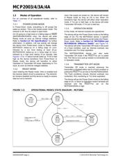
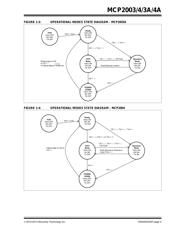
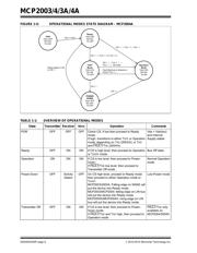
threshold (see Figure 1-1).
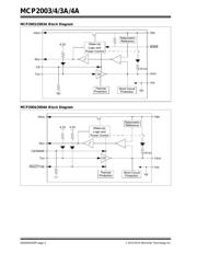
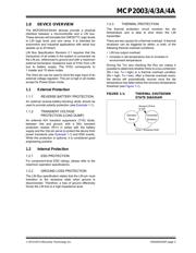
FIGURE 1-1: THERMAL SHUTDOWN
STATE DIAGRAM
Operation
Mode
Transmitter
Shutdown
LIN bus
Shorted
to V
BB
Tem p < S hu td ow nTEMP
器件 Datasheet 文档搜索
AiEMA 数据库涵盖高达 72,405,303 个元件的数据手册,每天更新 5,000 多个 PDF 文件
