Datasheet 搜索 > CAN芯片 > Microchip(微芯) > MCP2515T-I/ST 数据手册 > MCP2515T-I/ST 其他数据使用手册 3/94 页
 器件3D模型
¥ 5.326
MCP2515T-I/ST 其他数据使用手册 - Microchip(微芯)
制造商:
Microchip(微芯)
分类:
CAN芯片
封装:
TSSOP-20
描述:
MICROCHIP MCP2515T-I/ST. 芯片, CAN总线控制器, 1MBPS, 4/3, 5.5V, TSSOP-20
Pictures:
3D模型
符号图
焊盘图
引脚图
产品图
页面导航:
引脚图在P4P57Hot
原理图在P3P5P6P25P33
标记信息在P79
封装信息在P79P81P82P83P86P91
导航目录
MCP2515T-I/ST数据手册
Page:
of 94 Go
若手册格式错乱,请下载阅览PDF原文件
2003-2016 Microchip Technology Inc.
DS20001801H-page 3
MCP2515
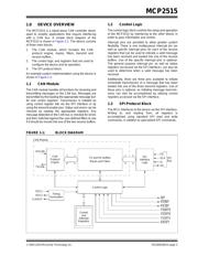
1.0 DEVICE OVERVIEW
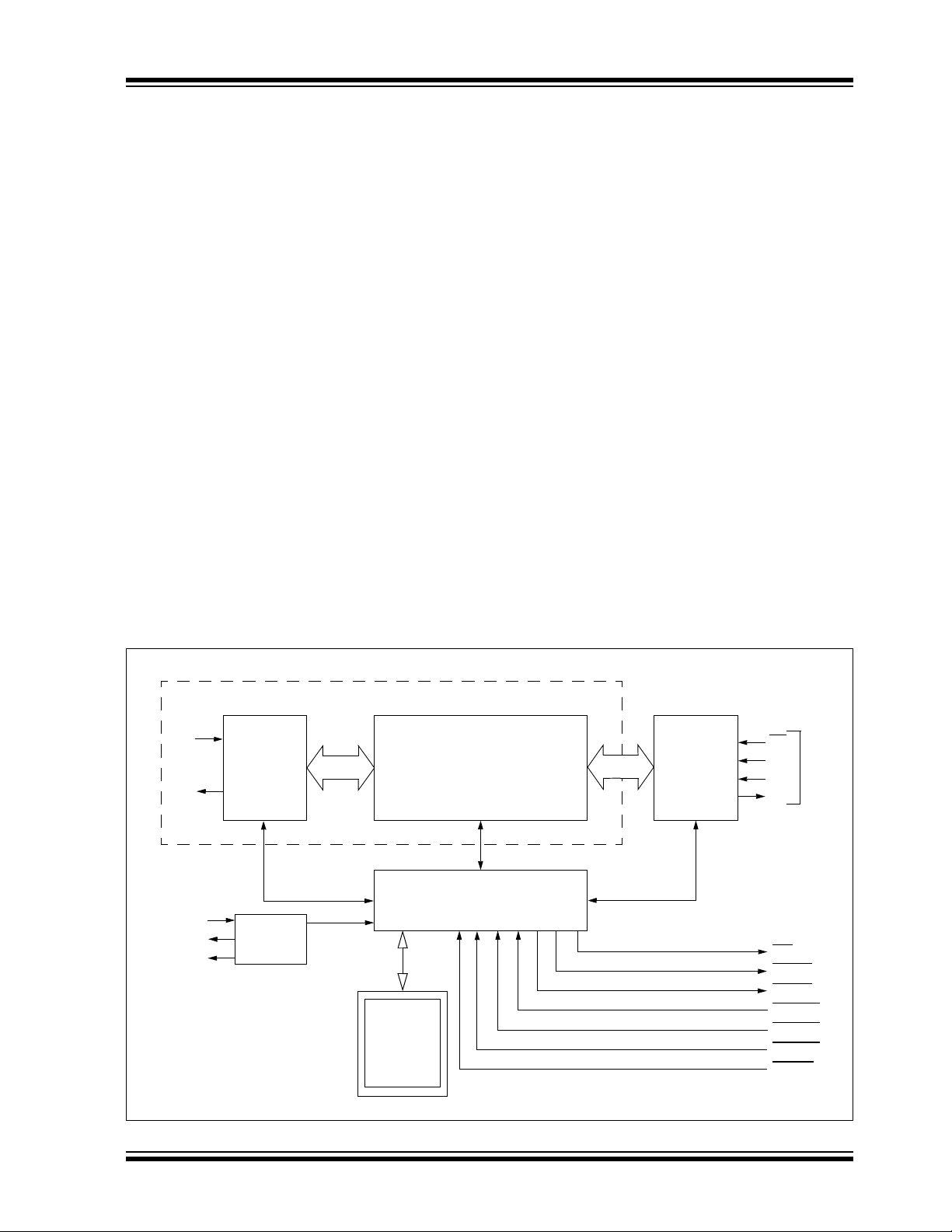
The MCP2515 is a stand-alone CAN controller devel-
oped to simplify applications that require interfacing
with a CAN bus. A simple block diagram of the
MCP2515 is shown in Figure 1-1. The device consists
of three main blocks:
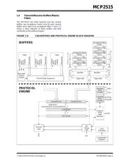
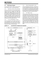
1. The CAN module, which includes the CAN
protocol engine, masks, filters, transmit and
receive buffers.
2. The control logic and registers that are used to
configure the device and its operation.
3. The SPI protocol block.
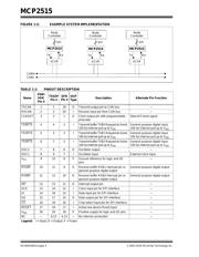
An example system implementation using the device is
shown in Figure 1-2.
1.1 CAN Module
The CAN module handles all functions for receiving and
transmitting messages on the CAN bus. Messages are
transmitted by first loading the appropriate message buf-
fer and control registers. Transmission is initiated by
using control register bits via the SPI interface or by
using the transmit enable pins. Status and errors can be
checked by reading the appropriate registers. Any
message detected on the CAN bus is checked for errors
and then matched against the user-defined filters to see
if it should be moved into one of the two receive buffers.
1.2 Control Logic
The control logic block controls the setup and operation
of the MCP2515 by interfacing to the other blocks in
order to pass information and control.
Interrupt pins are provided to allow greater system
flexibility. There is one multipurpose interrupt pin (as
well as specific interrupt pins) for each of the receive
registers that can be used to indicate a valid message
has been received and loaded into one of the receive
buffers. Use of the specific interrupt pins is optional.
The general purpose interrupt pin, as well as status
registers (accessed via the SPI interface), can also be
used to determine when a valid message has been
received.
Additionally, there are three pins available to initiate
immediate transmission of a message that has been
loaded into one of the three transmit registers. Use of
these pins is optional, as initiating message transmis-
sions can also be accomplished by utilizing control
registers accessed via the SPI interface.
1.3 SPI Protocol Block
The MCU interfaces to the device via the SPI interface.
Writing to, and reading from, all registers is
accomplished using standard SPI read and write
commands, in addition to specialized SPI commands.
FIGURE 1-1: BLOCK DIAGRAM
SPI
Interface
Logic
SPI
Bus
INT
CS
SCK
SI
SO
CAN
Protocol
Engine
RXCAN
TXCAN
Control Logic
RX0BF
RX1BF
TX0RTS
TX1RTS
TX2RTS
TX and RX Buffers
Masks and Filters
CAN Module
RESET
Timing
Generation
OSC1
OSC2
CLKOUT
Control
and
Interrupt
Registers
器件 Datasheet 文档搜索
AiEMA 数据库涵盖高达 72,405,303 个元件的数据手册,每天更新 5,000 多个 PDF 文件
