Datasheet 搜索 > DA转换器 > Microchip(微芯) > MCP4725A1T-E/CH 数据手册 > MCP4725A1T-E/CH 产品手册 3/50 页

¥ 4.682
MCP4725A1T-E/CH 产品手册 - Microchip(微芯)
制造商:
Microchip(微芯)
分类:
DA转换器
封装:
SOT-23-6
描述:
MCP4725 系列 12 位数字至模拟转换器### 数模转换器 - Microchip
Pictures:
3D模型
符号图
焊盘图
引脚图
产品图
页面导航:
引脚图在P13Hot
典型应用电路图在P33P34
原理图在P1
标记信息在P43
封装信息在P43P47
功能描述在P19
技术参数、封装参数在P4P5P30P31
应用领域在P1P33
电气规格在P4P5P19P30P31

导航目录
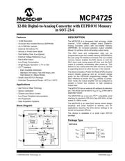
MCP4725A1T-E/CH数据手册
Page:
of 50 Go
若手册格式错乱,请下载阅览PDF原文件

© 2009 Microchip Technology Inc. DS22039D-page 3
MCP4725
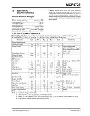
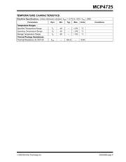
1.0 ELECTRICAL
CHARACTERISTICS
Absolute Maximum Ratings†
V
DD
...................................................................................6.5V
All inputs and outputs w.r.t V
SS
.................–0.3V to V
DD
+0.3V
Current at Input Pins ....................................................±2 mA
Current at Supply Pins ...............................................±50 mA
Current at Output Pins ...............................................±25 mA
Storage Temperature ...................................-65°C to +150°C
Ambient Temp. with Power Applied .............-55°C to +125°C
ESD protection on all pins ................ ≥ 6kV HBM, ≥ 400V MM
Maximum Junction Temperature (T
J
) ......................... +150°C
† Notice: Stresses above those listed under “Maximum
ratings” may cause permanent damage to the device. This is
a stress rating only and functional operation of the device at
these or any other conditions above those indicated in the
operation listings of this specification is not implied. Exposure
to maximum rating conditions for extended periods may affect
device reliability
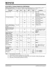
ELECTRICAL CHARACTERISTICS
Electrical Specifications: Unless otherwise indicated, all parameters apply at V
DD
= + 2.7V to 5.5V, V
SS
= 0V,
R
L
= 5 kΩ from V
OUT
to V
SS
, C
L
= 100 pF, T
A
= -40°C to +125°C. Typical values are at +25°C.
Parameter Sym Min Typ Max Units Conditions
Power Requirements
Operating Voltage V
DD
2.7 5.5 V
Supply Current I
DD
— 210 400 µA Digital input pins are
grounded, Output pin (V
OUT
)
is not connected (unloaded),
Code = 000h
Power-Down Current I
DDP
—0.06 2.0 µA V
DD
= 5.5V
Power-On-Reset
Threshold Voltage
V
POR
—2 — V
DC Accuracy
Resolution n 12 — — Bits Code Range = 000h to FFFh
INL Error INL — ±2 ±14.5 LSB Note 1
DNL DNL -0.75 ±0.2 ±0.75 LSB Note 1
Offset Error V
OS
0.02 0.75 % of FSR Code = 000h
Offset Error Drift ΔV
OS
/°C — ±1 — ppm/°C -45°C to +25°C
— ±2 — ppm/°C +25°C to +85°C
Gain Error G
E
-2 -0.1 2 % of FSR Code = FFFh,
Offset error is not included.
Gain Error Drift ΔG
E
/°C — -3 — ppm/°C
Output Amplifier
Phase Margin
p
M
— 66 — Degree(°) C
L
= 400 pF, R
L
= ∞
Capacitive Load Stability C
L
— — 1000 pF R
L
= 5 kΩ, Note 2
Slew Rate SR — 0.55 — V/µs
Short Circuit Current I
SC
—15 24 mA V
DD
= 5V, V
OUT
= Grounded
Output Voltage Settling
Time
T
S
—6 — µsNote 3
Note 1: Test Code Range: 100 to 4000.
2: This parameter is ensure by design and not 100% tested.
3: Within 1/2 LSB of the final value when code changes from 1/4 to 3/4 (400h to C00h) of full scale range.
4: Logic state of external address selection pin (A0 pin).
器件 Datasheet 文档搜索
AiEMA 数据库涵盖高达 72,405,303 个元件的数据手册,每天更新 5,000 多个 PDF 文件
