Datasheet 搜索 > Microchip(微芯) > MIC28510-5V-EV 数据手册 > MIC28510-5V-EV 其他数据使用手册 2/14 页


¥ 227.7
MIC28510-5V-EV 其他数据使用手册 - Microchip(微芯)
制造商:
Microchip(微芯)
Pictures:
3D模型
符号图
焊盘图
引脚图
产品图
页面导航:
原理图在P4P8
型号编码规则在P1
功能描述在P1
导航目录
MIC28510-5V-EV数据手册
Page:
of 14 Go
若手册格式错乱,请下载阅览PDF原文件
Micrel, Inc. MIC28510 4A Evaluation Board
Features
March 2012
2
M9999-030712
hbwhelp@micrel.com
or (408) 955-1690
MIC28510 evaluation
board, which is preset to 3.3V, is determined by the
feedback divider, shown in Equation 1:
Feedback Resistors
The output voltage on the
⎟
⎟
⎠
⎜
⎜
⎝
+×=
BOTTOM
REFOUT
R
R4
1VV
where V
REF
= 0.8V, and R
BOTTOM
is one o
which corresponds
⎞⎛
Eq. 1
f R5-R12,
to 0.9V, 1.0V, 1.2V, 1.5V, 1.8V,
2.5V, 3.3V, or 5V. Leaving the R
BOTTOM
open gives a
0.8V output voltage. All
above can be set by modifying R
BOTTOM
alu
according to Equation 2:
other voltages not listed
v e
REFOUT
REF
BOTTOM
VV
R
−
=
Note that the output voltage should not be
VR4×
Eq. 2
5V due to the 6.3V voltage rating o
mmended
hown in the MIC28510 12V/4A
e output
d for 12V
ode
ng the
t critical
nt limit
om FET.
t of
easurement
The resistor, R13, is placed in series with the reg
feedback path. The control loop gain can be
measured by connecting an impedance analyzer
across the resistor and selecting the resistor value in
between 20Ω to 50Ω.
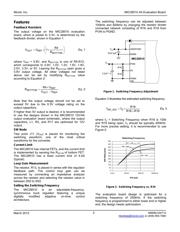
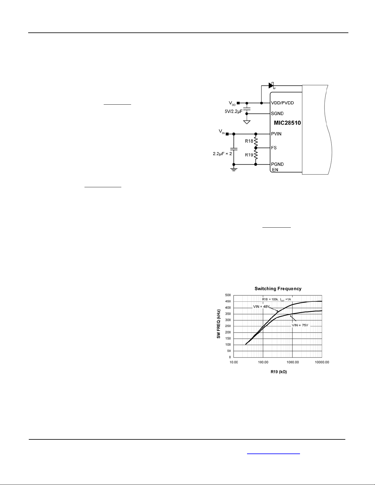
Setting the Switching Frequency
The MIC28510 is an adjustable-frequency,
synchronous buck regulator featuring a unique
digitally modified adaptive on-time control
architecture.
be adjusted between
ng the resistor divider
connected network consisting of R18 and R19 from
PVIN to PGND.
The switching frequency can
100kHz and 500kHz by changi
Figure 1. Switching Frequency Adjustment
switching frequency:
Equation 3 illustrates the estimated
set to
n the exceed
R19R18
R19
ff
OSW_ADJ
+
×=
output capacitors.
If higher than 5V output is desired, it is reco
to use the designs s
Eq. 3
where f
O
= Switching Frequency when R18 is 100k
and R19 being open, f
O
should be typically 450kHz.
For more precise setting, it is recommended to use
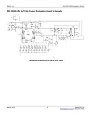
Figure 2:
output evaluation board schematic, where th
capacitors, L1, R3, and R17 are optimize
output.
SW N
Test point J11 (V
SW
) is placed for monitori
switching waveform, one of the mos
waveforms for the converter.
Current Limit
The MIC28510 has internal FETs, and the curre
is implemented by sensing the R
DS-ON
of bott
The MIC28510 has a fixed current limi
(typical).
Loop Gain M
6.5A
ulator
Figure 2. Switching Frequency vs. R19
The evaluation board design is optimized for a
switching frequency of 250kHz. If the switching
frequency is programmed to either lower end or higher
end, the design needs optimization.
器件 Datasheet 文档搜索
AiEMA 数据库涵盖高达 72,405,303 个元件的数据手册,每天更新 5,000 多个 PDF 文件
