Datasheet 搜索 > 逻辑芯片 > Fairchild(飞兆/仙童) > MM74HC86MX 数据手册 > MM74HC86MX 其他数据使用手册 1/18 页

 器件3D模型
¥ 0.178
MM74HC86MX 其他数据使用手册 - Fairchild(飞兆/仙童)
制造商:
Fairchild(飞兆/仙童)
分类:
逻辑芯片
封装:
SOIC-14
描述:
FAIRCHILD SEMICONDUCTOR MM74HC86MX 异或门, HC系列, CMOS, 2输入, 4门, 2V至6V, NSOIC-14
Pictures:
3D模型
符号图
焊盘图
引脚图
产品图
页面导航:
引脚图在P2Hot
典型应用电路图在P9P12P13
原理图在P2
封装尺寸在P14P15P16P17
型号编码规则在P1
封装信息在P1
功能描述在P1
技术参数、封装参数在P3
电气规格在P3P4P5P6P7
导航目录
MM74HC86MX数据手册
Page:
of 18 Go
若手册格式错乱,请下载阅览PDF原文件
© 2003 Fairchild Semiconductor Corporation DS005352 www.fairchildsemi.com
February 1984
Revised October 2003
MM74HC4046 CMOS Phase Lock Loop
MM74HC4046
CMOS Phase Lock Loop
General Description
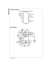
The MM74HC4046 is a low power phase lock loop utilizing
advanced silicon-gate CMOS technology to obtain high fre-
quency operation both in the phase comparator and VCO
sections. This device contains a low power linear voltage
controlled oscillator (VCO), a source follower, and three
phase comparators. The three phase comparators have a
common signal input and a common comparator input. The
signal input has a self biasing amplifier allowing signals to
be either capacitively coupled to the phase comparators
with a small signal or directly coupled with standard input
logic levels. This device is similar to the CD4046 except
that the Zener diode of the metal gate CMOS device has
been replaced with a third phase comparator.
Phase Comparator I is an exclusive OR (XOR) gate. It pro-
vides a digital error signal that maintains a 90 phase shift
between the VCO’s center frequency and the input signal
(50% duty cycle input waveforms). This phase detector is
more susceptible to locking onto harmonics of the input fre-
quency than phase comparator I, but provides better noise
rejection.
Phase comparator III is an SR flip-flop gate. It can be used
to provide the phase comparator functions and is similar to
the first comparator in performance.
Phase comparator II is an edge sensitive digital sequential
network. Two signal outputs are provided, a comparator
output and a phase pulse output. The comparator output is
a 3-STATE output that provides a signal that locks the VCO
output signal to the input signal with 0 phase shift between
them. This comparator is more susceptible to noise throw-
ing the loop out of lock, but is less likely to lock onto har-
monics than the other two comparators.
In a typical application any one of the three comparators
feed an external filter network which in turn feeds the VCO
input. This input is a very high impedance CMOS input
which also drives the source follower. The VCO’s operating
frequency is set by three external components connected
to the C1A, C1B, R1 and R2 pins. An inhibit pin is provided
to disable the VCO and the source follower, providing a
method of putting the IC in a low power state.
The source follower is a MOS transistor whose gate is con-
nected to the VCO input and whose drain connects the
Demodulator output. This output normally is used by tying
a resistor from pin 10 to ground, and provides a means of
looking at the VCO input without loading down modifying
the characteristics of the PLL filter.
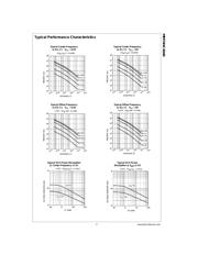
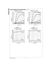
Features
■ Low dynamic power consumption: (V
CC
= 4.5V)
■ Maximum VCO operating frequency:
12 MHz (V
CC
= 4.5V)
■ Fast comparator response time (V
CC
= 4.5V)
Comparator I: 25 ns
Comparator II: 30 ns
Comparator III: 25 ns
■ VCO has high linearity and high temperature stability
Ordering Code:
Devices also available in Tape and Reel. Specify by appending the suffix letter “X” to the ordering code.
Order Number Package Number Package Description
MM74HC4046M M16A 16-Lead Small Outline Integrated Circuit (SOIC), JEDEC MS-012, 0.150" Narrow
MM74HC4046SJ M16D 16-Lead Small Outline Package (SOP), EIAJ TYPE II, 5.3mm Wide
MM74HC4046MTC MTC16 16-Lead Thin Shrink Small Outline Package (TSSOP), JEDEC MO-153, 4.4mm Wide
MM74HC4046N N16E 16-Lead Plastic Dual-In-Line Package (PDIP), JEDEC MS-001, 0.300" Wide
器件 Datasheet 文档搜索
AiEMA 数据库涵盖高达 72,405,303 个元件的数据手册,每天更新 5,000 多个 PDF 文件
