Datasheet 搜索 > 微处理器 > NXP(恩智浦) > MPC8308CVMAGD 数据手册 > MPC8308CVMAGD 产品描述及参数 6/83 页

¥ 781.411
MPC8308CVMAGD 产品描述及参数 - NXP(恩智浦)
制造商:
NXP(恩智浦)
分类:
微处理器
封装:
BGA-473
描述:
NXP MPC8308CVMAGD 芯片, 微处理器, 32位, 400MHZ, MAPBGA-473
Pictures:
3D模型
符号图
焊盘图
引脚图
产品图
页面导航:
原理图在P2
封装尺寸在P59P60
型号编码规则在P80P81
标记信息在P81
技术参数、封装参数在P3P8P9P11P12P13P15P17P18P19P20P21
电气规格在P2P3P4P5P7P8P9P10P11P15P16P17
型号编号列表在P80
导航目录
MPC8308CVMAGD数据手册
Page:
of 83 Go
若手册格式错乱,请下载阅览PDF原文件
MPC8308 PowerQUICC II Pro Processor Hardware Specification, Rev. 3
6 Freescale Semiconductor
Power Characteristics
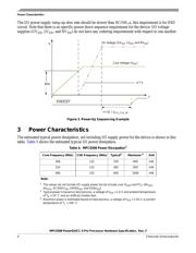
The I/O power supply ramp-up slew rate should be slower than 4V/100 s, this requirement is for ESD
circuit. Note that there is no specific power down sequence requirement for the device. I/O voltage
supplies (GV
DD
, LV
DD
, and NV
DD
) do not have any ordering requirements with respect to one another.
Figure 3. Power-Up Sequencing Example
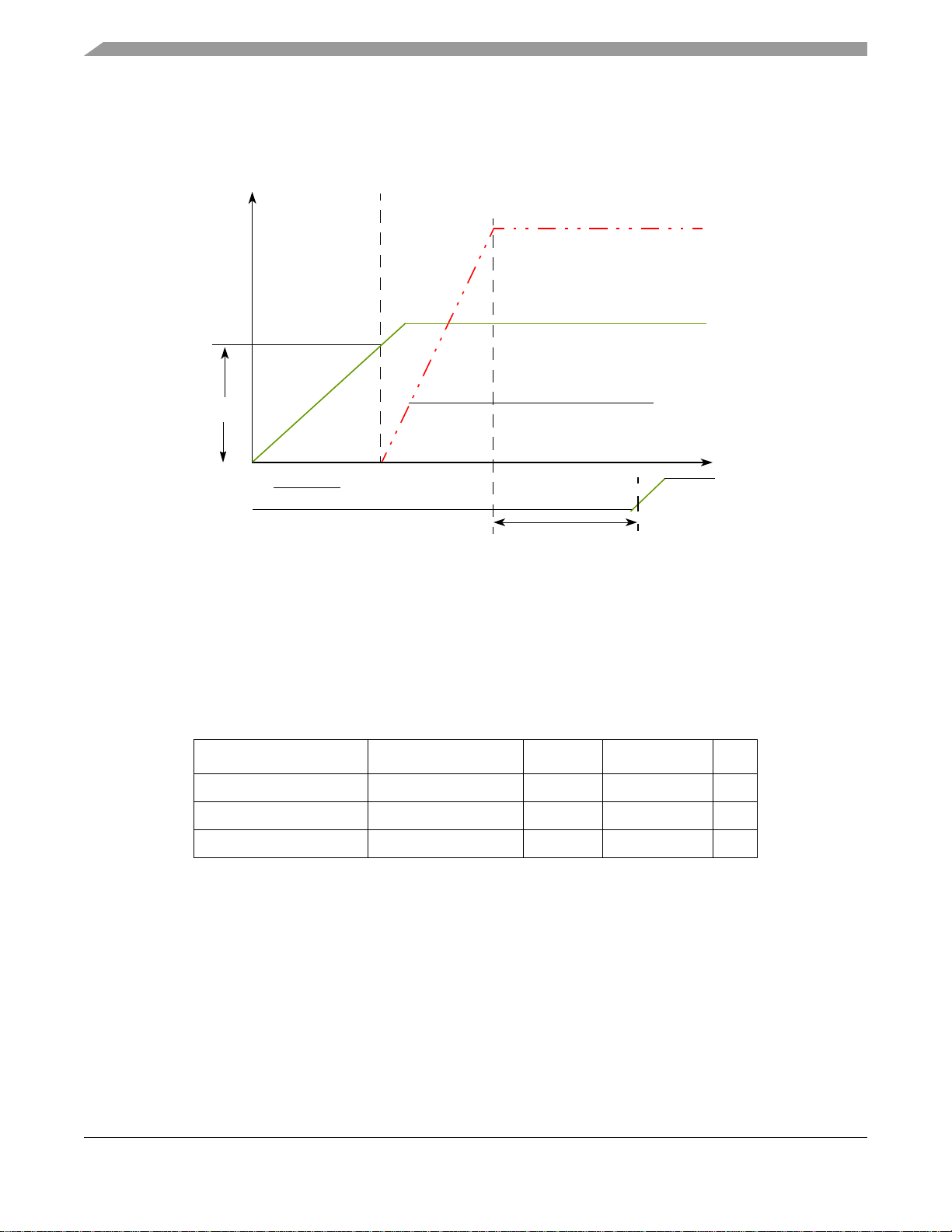
3 Power Characteristics
The estimated typical power dissipation, not including I/O supply power for the device is shown in this
table. Table 5 shows the estimated typical I/O power dissipation.
Table 4. MPC8308 Power Dissipation
1
1
The values do not include I/O supply power but do include core (V
DD
) and PLL (AV
DD1,
AV
DD2
, XCOREV
DD
, XPADV
DD
, and SDAV
DD
)
Core Frequency (MHz) CSB Frequency (MHz) Typical
2
2
Typical power is based on best process, a voltage of V
DD
= 1.0 V and ambient temperature
of T
A
= 25 C and an artificial smoker test.
Maximum
3
3
Maximum power is estimated based on best process, a voltage of V
DD
= 1.05 V, a junction
temperature of T
J
= 105 C
Unit
266 133 530 900 mW
333 133 565 950 mW
400 133 600 1000 mW
Note:
t
90%
V
Core Voltage (V
DD
)
I/O Voltage (GV
DD
, LV
DD
, and NV
DD
)
0
0.7 V
PORESET
>= 32 t
SYS_CLK_IN
器件 Datasheet 文档搜索
AiEMA 数据库涵盖高达 72,405,303 个元件的数据手册,每天更新 5,000 多个 PDF 文件
