Datasheet 搜索 > 微处理器 > Freescale(飞思卡尔) > MPC8308VMAGD 数据手册 > MPC8308VMAGD 产品描述及参数 3/96 页
 器件3D模型
¥ 7.181
MPC8308VMAGD 产品描述及参数 - Freescale(飞思卡尔)
制造商:
Freescale(飞思卡尔)
分类:
微处理器
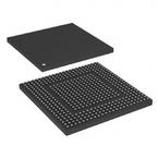
封装:
MAPBGA-473
描述:
微处理器 - MPU E300 MP PbFr 400
Pictures:
3D模型
符号图
焊盘图
引脚图
产品图
页面导航:
原理图在P2
封装尺寸在P59P60
型号编码规则在P80P81
标记信息在P81
技术参数、封装参数在P3P8P9P11P12P13P15P17P18P19P21P22
电气规格在P2P3P4P5P7P8P10P14P15P16P20P21
型号编号列表在P80

导航目录
MPC8308VMAGD数据手册
Page:
of 96 Go
若手册格式错乱,请下载阅览PDF原文件
MPC8308 PowerQUICC II Pro Processor Hardware Specification, Rev. 4
Freescale Semiconductor 3
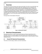
Electrical Characteristics
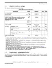
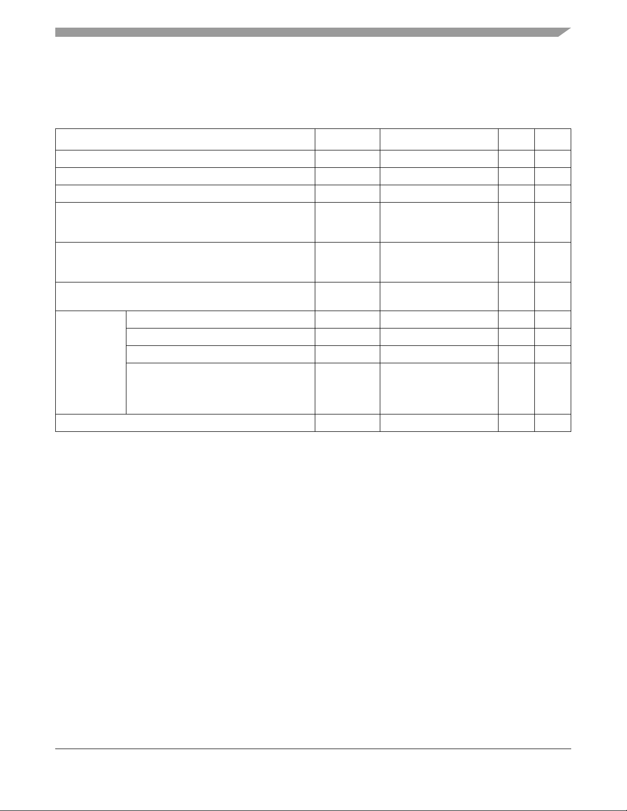
2.1.1 Absolute maximum ratings
This table lists the absolute maximum ratings.
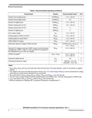
2.1.2 Power supply voltage specification
This table provides the recommended operating conditions for the device. Note that the values in this table
are the recommended and tested operating conditions. Proper device operation outside of these conditions
is not guaranteed.
Table 1. Absolute maximum ratings
1
Characteristic Symbol Max Value Unit Notes
Core supply voltage V
DD
–0.3 to 1.26 V —
PLL supply voltage AV
DD1,
AV
DD2
–0.3 to 1.26 V —
DDR2 DRAM I/O voltage GV
DD
–0.3 to 1.9 V —
Local bus, DUART, system control and power management,
eSDHC, I
2
C, USB, Interrupt, Ethernet management, SPI,
Miscellaneous and JTAG I/O voltage
NV
DD
–0.3 to 3.6 V 7
SerDes PHY XCOREV
DD
,
XPADV
DD
,
SDAV
DD
–0.3 to 1.26 V —
eTSEC I/O Voltage LV
DD1,
LV
DD2
–0.3 to 2.75 or
–0.3 to 3.6
V6, 8
Input voltage DDR2 DRAM signals MV
IN
–0.3 to (GV
DD
+ 0.3) V 2, 5
DDR2 DRAM reference MV
REF
–0.3 to (GV
DD
+ 0.3) V 2, 5
eTSEC LV
IN –0.3 to (LV
DD
+ 0.3) V 4, 5,8
Local bus, DUART, system control and power
management, eSDHC, I
2
C, Interrupt,
Ethernet management, SPI, Miscellaneous
and JTAG I/O voltage
OV
IN
–0.3 to (NV
DD
+ 0.3) V 3, 5,7
Storage temperature range T
STG
–55 to 150 C—
Notes:
1. Functional and tested operating conditions are given in Ta bl e 2 . Absolute maximum ratings are stress ratings only, and
functional operation at the maximums is not guaranteed. Stresses beyond those listed may affect device reliability or cause
permanent damage to the device.
2. Caution: MV
IN
must not exceed GV
DD
by more than 0.3 V. This limit may be exceeded for a maximum of 20 ms during
power-on reset and power-down sequences.
3. Caution: OV
IN
must not exceed NV
DD
by more than 0.3 V. This limit may be exceeded for a maximum of 20 ms during
power-on reset and power-down sequences.
4. Caution: LV
IN
must not exceed LV
DD
by more than 0.3 V. This limit may be exceeded for a maximum of 20 ms during
power-on reset and power-down sequences.
5. (M, L, O)V
IN
and MV
REF
may overshoot/undershoot to a voltage and for a maximum duration as shown in Figure 2
6. The max value of supply voltage should be selected based on the RGMII mode. The lower range applies to RGMII mode.
7. NV
DD
here refers to NV
DDA
, NV
DDB
,NV
DDG
, NV
DDH
, NV
DDJ
, NV
DDP_K
from the ball map.
8. LV
DD1
here refers to NV
DDC
and LV
DD2
refers to NV
DDF
from the ball map
器件 Datasheet 文档搜索
AiEMA 数据库涵盖高达 72,405,303 个元件的数据手册,每天更新 5,000 多个 PDF 文件
