Datasheet 搜索 > 微处理器 > NXP(恩智浦) > MPC8349EVVAGDB 数据手册 > MPC8349EVVAGDB 产品描述及参数 2/12 页

¥ 1159.037
MPC8349EVVAGDB 产品描述及参数 - NXP(恩智浦)
制造商:
NXP(恩智浦)
分类:
微处理器
封装:
TBGA-672
描述:
PowerPC系列 400MHz
Pictures:
3D模型
符号图
焊盘图
引脚图
产品图
MPC8349EVVAGDB数据手册
Page:
of 12 Go
若手册格式错乱,请下载阅览PDF原文件

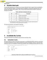
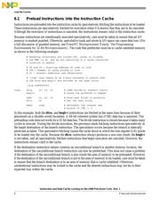
Instruction and Data Cache Locking on the e300 Processor Core, Rev. 1
2 Freescale Semiconductor
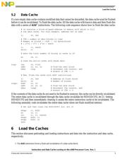
Overview of Cache Locking on the e300 Processor
cache is unlocked. When a cache is unlocked, all entries (including invalid entries) are available. Entire
cache locking is inefficient if the number of instructions or the size of data to be locked is small compared
to the cache size.
Way locking locks only a portion of the cache by locking ways within the cache. Locking always begins
with the first way (way0) and is sequential; that is, you can lock ways 0, 1, and 2 but not ways 0 and 2. At
least one way must be left unlocked. The maximum number of lockable ways is seven on the e300
processor (way0–way6).
Unlike entire cache locking, invalid entries in a locked way are accessible and available for data
placement. As hits to the cache fill invalid entries within a locked way, the entries become valid and
locked. This behavior differs from entire cache locking in which nothing is placed into the locked cache,
even if there are invalid entries in the cache. Unlocked ways of the cache behave normally.
2 Overview of Cache Locking on the e300 Processor
To lock the instruction cache, set the instruction cache enable bit HID0[ICE], bit 16. To lock the data cache,
set the data cache enable bit HID0[DCE], bit 17. The following assembly code enables the instruction and
data caches:
# Enable the instruction and data caches. This corresponds
# to setting the ICE and DCE bits in HID0 (bits 16 and 17)
mfspr r1, HID0
ori r1, r1, 0xc000
sync
mtspr HID0, r1
Two distinct memory areas must be set up to enable cache locking:
• The first area is where the locking code resides and is executed.
• The second area contains the data to be locked.
Both areas of memory must be in locations that are translated by the memory management unit (MMU).
This translation can be performed either with the page table
1
or the block address translation (BAT)
registers. This document describes the use of BAT register translations.
The instruction cache locking procedure is as follows; the remainder of this document discusses each of
these steps in detail:
1. Set up memory.
2. Disable interrupts.
3. Invalidate the entire cache to ensure known state and force placement to way0.
4. Load the cache with the data to be locked.
5. Lock the cache, either way or entire cache.
1. Issues arising from using page table address translation are beyond the scope of this document.
器件 Datasheet 文档搜索
AiEMA 数据库涵盖高达 72,405,303 个元件的数据手册,每天更新 5,000 多个 PDF 文件
