Datasheet 搜索 > 微控制器 > TI(德州仪器) > MSP430G2332QPW2EP 数据手册 > MSP430G2332QPW2EP 其他数据使用手册 1/12 页
 器件3D模型
¥ 12.751
MSP430G2332QPW2EP 其他数据使用手册 - TI(德州仪器)
制造商:
TI(德州仪器)
分类:
微控制器
封装:
TSSOP-20
描述:
16位微控制器 - MCU Mixed Signal MCU
Pictures:
3D模型
符号图
焊盘图
引脚图
产品图
页面导航:
封装尺寸在P9P10
型号编码规则在P8
功能描述在P1P12
技术参数、封装参数在P1P2P12

导航目录
MSP430G2332QPW2EP数据手册
Page:
of 12 Go
若手册格式错乱,请下载阅览PDF原文件
SQJ960EP
www.vishay.com
Vishay Siliconix
S15-1878-Rev. D, 17-Aug-15
1
Document Number: 67017
For technical questions, contact: automostechsupport@vishay.com
THIS DOCUMENT IS SUBJECT TO CHANGE WITHOUT NOTICE. THE PRODUCTS DESCRIBED HEREIN AND THIS DOCUMENT
ARE SUBJECT TO SPECIFIC DISCLAIMERS, SET FORTH AT www.vishay.com/doc?91000
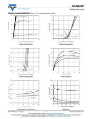
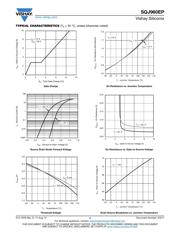
Automotive Dual N-Channel 60 V (D-S) 175 °C MOSFET
FEATURES
• TrenchFET
®
power MOSFET
• AEC-Q101 qualified
• 100 % R
g
and UIS tested
• Material categorization:
for definitions of compliance please see
www.vishay.com/doc?99912
Notes
a. Package limited.
b. Pulse test; pulse width ≤ 300 μs, duty cycle ≤ 2 %.
c. When mounted on 1" square PCB (FR4 material).
d. See solder profile (www.vishay.com/doc?73257
). The PowerPAK SO-8L is a leadless package. The end of the lead terminal is exposed
copper (not plated) as a result of the singulation process in manufacturing. A solder fillet at the exposed copper tip cannot be guaranteed
and is not required to ensure adequate bottom side solder interconnection.
e. Rework conditions: manual soldering with a soldering iron is not recommended for leadless components.
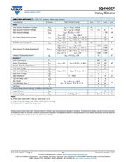
PRODUCT SUMMARY
V
DS
(V) 60
R
DS(on)
(Ω) at V
GS
= 10 V 0.036
R
DS(on)
(Ω) at V
GS
= 4.5 V 0.046
I
D
(A) per leg 8
Configuration Dual
Package PowerPAK SO-8L
PowerPAK
®
SO-8L Dual
Top View
1
6.15 mm
5.13 mm
1
6.15
m
m
5
.13
m
m
Bottom View
2
G
1
3
S
2
4
G
2
1
S
1
D
2
D
1
N-Channel MOSFET
D
1
G
1
S
1
N-Channel MOSFET
D
2
G
2
S
2
ABSOLUTE MAXIMUM RATINGS (T
C
= 25 °C, unless otherwise noted)
PARAMETER SYMBOL LIMIT UNIT
Drain-Source Voltage V
DS
60
V
Gate-Source Voltage V
GS
± 20
Continuous Drain Current
a
T
C
= 25 °C
I
D
8
A
T
C
= 125 °C 8
Continuous Source Current (Diode Conduction)
a
I
S
8
Pulsed Drain Current
b
I
DM
32
Single Pulse Avalanche Current
L = 0.1 mH
I
AS
16
Single Pulse Avalanche Energy E
AS
12 mJ
Maximum Power Dissipation
b
T
C
= 25 °C
P
D
34
W
T
C
= 125 °C 11
Operating Junction and Storage Temperature Range T
J
, T
stg
-55 to +175
°C
Soldering Recommendations (Peak Temperature)
d, e
260
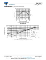
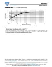
THERMAL RESISTANCE RATINGS
PARAMETER SYMBOL LIMIT UNIT
Junction-to-Ambient PCB Mount
c
R
thJA
85
°C/W
Junction-to-Case (Drain) R
thJC
4.3
器件 Datasheet 文档搜索
AiEMA 数据库涵盖高达 72,405,303 个元件的数据手册,每天更新 5,000 多个 PDF 文件
