Datasheet 搜索 > RAM芯片 > Micron(镁光) > MT41K256M16TW-107 IT:P 数据手册 > MT41K256M16TW-107 IT:P 其他数据使用手册 1/218 页

¥ 5.607
MT41K256M16TW-107 IT:P 其他数据使用手册 - Micron(镁光)
制造商:
Micron(镁光)
分类:
RAM芯片
封装:
FBGA-96
描述:
SDRAM, 256M x 16bit, 2048Byte, 1.07ns, 并行接口, FBGA-96
Pictures:
3D模型
符号图
焊盘图
引脚图
产品图
页面导航:
原理图在P15P16P153
封装尺寸在P23P24P25P26P27P28
标记信息在P1P2
功能描述在P13P14P153P199
技术参数、封装参数在P29P30P33P34P35P36P37P38P39P40P41P42
应用领域在P11
电气规格在P29P30P33P34P35P36P37P38P39P40P41P42
型号编号列表在P2
导航目录
MT41K256M16TW-107 IT:P数据手册
Page:
of 218 Go
若手册格式错乱,请下载阅览PDF原文件
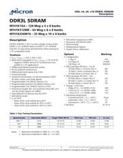
DDR3L SDRAM
MT41K1G4 – 128 Meg x 4 x 8 banks
MT41K512M8 – 64 Meg x 8 x 8 banks
MT41K256M16 – 32 Meg x 16 x 8 banks
Description
DDR3L SDRAM (1.35V) is a low voltage version of the
DDR3 (1.5V) SDRAM. Refer to DDR3 (1.5V) SDRAM
(Die Rev :E) data sheet specifications when running in
1.5V compatible mode.
Features
•V
DD
= V
DDQ
= 1.35V (1.283–1.45V)
• Backward compatible to V
DD
= V
DDQ
= 1.5V ±0.075V
– Supports DDR3L devices to be backward com-
patible in 1.5V applications
• Differential bidirectional data strobe
•8n-bit prefetch architecture
• Differential clock inputs (CK, CK#)
• 8 internal banks
• Nominal and dynamic on-die termination (ODT)
for data, strobe, and mask signals
• Programmable CAS (READ) latency (CL)
• Programmable posted CAS additive latency (AL)
• Programmable CAS (WRITE) latency (CWL)
• Fixed burst length (BL) of 8 and burst chop (BC) of 4
(via the mode register set [MRS])
• Selectable BC4 or BL8 on-the-fly (OTF)
• Self refresh mode
•T
C
of 105°C
– 64ms, 8192-cycle refresh up to 85°C
– 32ms, 8192-cycle refresh at >85°C to 95°C
– 16ms, 8192-cycle refresh at >95°C to 105°C
• Self refresh temperature (SRT)
• Automatic self refresh (ASR)
• Write leveling
• Multipurpose register
• Output driver calibration
Options Marking
• Configuration
– 1 Gig x 4 1G4
– 512 Meg x 8 512M8
– 256 Meg x 16 256M16
• FBGA package (Pb-free) – x4, x8
– 78-ball (9mm x 10.5mm) Rev. E RH
– 78-ball (7.5mm x 10.6mm) Rev. N RG
– 78-ball (8mm x 10.5mm) Rev. P DA
• FBGA package (Pb-free) – x16
– 96-ball (9mm x 14mm) Rev. E HA
– 96-ball (7.5mm x 13.5mm) Rev. N LY
– 96-ball (8mm x 14mm) Rev. P TW
• Timing – cycle time
– 938ps @ CL = 14 (DDR3-2133) -093
– 1.07ns @ CL = 13 (DDR3-1866) -107
– 1.25ns @ CL = 11 (DDR3-1600) -125
• Operating temperature
– Commercial (0°C T
C
+95°C) None
– Industrial (–40°C T
C
+95°C) IT
– Automotive (–40°C T
C
+105°C) AT
• Revision :E/:N/:P
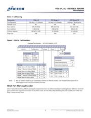
Table 1: Key Timing Parameters
Speed Grade Data Rate (MT/s) Target
t
RCD-
t
RP-CL
t
RCD (ns)
t
RP (ns) CL (ns)
-093
1, 2
2133 14-14-14 13.09 13.09 13.09
-107
1
1866 13-13-13 13.91 13.91 13.91
-125 1600 11-11-11 13.75 13.75 13.75
Notes:
1. Backward compatible to 1600, CL = 11 (-125).
2. Backward compatible to 1866, CL = 13 (-107).
4Gb: x4, x8, x16 DDR3L SDRAM
Description
09005aef85af8fa8
4Gb_DDR3L.pdf - Rev. R 09/18 EN
1
Micron Technology, Inc. reserves the right to change products or specifications without notice.
© 2017 Micron Technology, Inc. All rights reserved.
Products and specifications discussed herein are subject to change by Micron without notice.
器件 Datasheet 文档搜索
AiEMA 数据库涵盖高达 72,405,303 个元件的数据手册,每天更新 5,000 多个 PDF 文件
