Datasheet 搜索 > New Jersey Semiconductor > MTP3055E 数据手册 > MTP3055E 其他数据使用手册 1/4 页


¥ 0
MTP3055E 其他数据使用手册 - New Jersey Semiconductor
制造商:
New Jersey Semiconductor
Pictures:
3D模型
符号图
焊盘图
引脚图
产品图
MTP3055E数据手册
Page:
of 4 Go
若手册格式错乱,请下载阅览PDF原文件
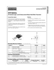
MTP3055VL
MTP3055VL Rev. A1
MTP3055VL
N-Channel Logic Level Enhancement Mode Field Effect Transistor
General Description
This N-Channel Logic Level MOSFET has been designed
specifically for low voltage, high speed switching
applications i.e. power supplies and power motor
controls.
This MOSFET features faster switching and lower gate
charge than other MOSFETs with comparable R
DS(ON)
specifications.
The result is a MOSFET that is easy and safer to drive
(even at very high frequencies).
June 2000
DISTRIBUTION GROUP*
Features
• 12 A, 60 V. R
DS(ON)
= 0.18 Ω @ V
GS
= 5 V
• Critical DC electrical parameters specified at elevated
temperature.
• Low drive requirements allowing operation directly from
logic drivers. Vgs(th) < 2 V.
• Rugged internal source-drain diode can eliminate the
need for an external Zener diode transient suppressor.
• 175°C maximum junction temperature rating.
1999 Fairchild Semiconductor Corporation
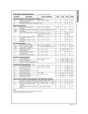
Absolute Maximum Ratings
T
C
= 25°C unless otherwise noted
Symbol Parameter
Ratings
Units
V
DSS
Drain-Source Voltage 60 V
V
GSS
Gate-Source Voltage
±
15 V
I
D
Drain Current - Continuous 12 A
- Pulsed 42
Power Dissipation @ T
C
= 25
°
C48WP
D
Derate above 25
°
C0.32W/
°
C
T
J
, T
STG
Operating and Storage Junction Temperature Range -65 to +175
°
C
Thermal Characteristics
R
θ
JC
Thermal Resistance, Junction-to- Case 3.13
°
C/W
R
θ
JA
Thermal Resistance, Junction-to- Ambient
(Note 1)
62.5
°
C/W
Package Outlines and Ordering Information
Device Marking Device Package Information Quantity
MTP3055VL MTP3055VL Rails/Tubes 45 units
*
Die and manufacturing source subject to change without prior notification
.
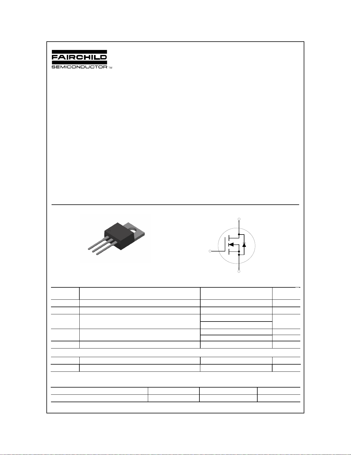
S
G
D
TO-220
S
D
G
器件 Datasheet 文档搜索
AiEMA 数据库涵盖高达 72,405,303 个元件的数据手册,每天更新 5,000 多个 PDF 文件
