Datasheet 搜索 > 存储芯片 > ST Microelectronics(意法半导体) > NAND01GW3B2AN6E 数据手册 > NAND01GW3B2AN6E 其他数据使用手册 1/60 页
 器件3D模型
¥ 16.668
NAND01GW3B2AN6E 其他数据使用手册 - ST Microelectronics(意法半导体)
制造商:
ST Microelectronics(意法半导体)
分类:
存储芯片
封装:
TSOP-48
描述:
NAND闪存 2.7-3.6V 1G (128Mx8)
Pictures:
3D模型
符号图
焊盘图
引脚图
产品图
页面导航:
典型应用电路图在P9P14
型号编码规则在P7P58
技术参数、封装参数在P40
导航目录
NAND01GW3B2AN6E数据手册
Page:
of 60 Go
若手册格式错乱,请下载阅览PDF原文件
April 2008 Rev 5 1/60
1
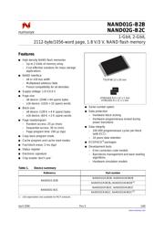
NAND01G-B2B
NAND02G-B2C
1-Gbit, 2-Gbit,
2112-byte/1056-word page, 1.8 V/3 V, NAND flash memory
Features
■ High density NAND flash memories
– Up to 2 Gbits of memory array
– Cost effective solutions for mass storage
applications
■ NAND interface
– x8 or x16 bus width
– Multiplexed address/ data
– Pinout compatibility for all densities
■ Supply voltage: 1.8 V/3.0 V
■ Page size
– x8 device: (2048 + 64 spare) bytes
– x16 device: (1024 + 32 spare) words
■ Block size
– x8 device: (128 K + 4 K spare) bytes
– x16 device: (64 K + 2 K spare) words
■ Page read/program
– Random access: 25 µs (max)
– Sequential access: 30 ns (min)
– Page program time: 200 µs (typ)
■ Copy back program mode
■ Cache program and cache read modes
■ Fast block erase: 2 ms (typ)
■ Status register
■ Electronic signature
■ Chip enable ‘don’t care’
■ Serial number option
■ Data protection
– Hardware block locking
– Hardware program/erase locked during
power transitions
■ Data integrity
– 100 000 program/erase cycles per block
(with ECC)
– 10 years data retention
■ ECOPACK
®
packages
■ Development tools
– Error correction code models
– Bad blocks management and wear leveling
algorithms
– Hardware simulation models
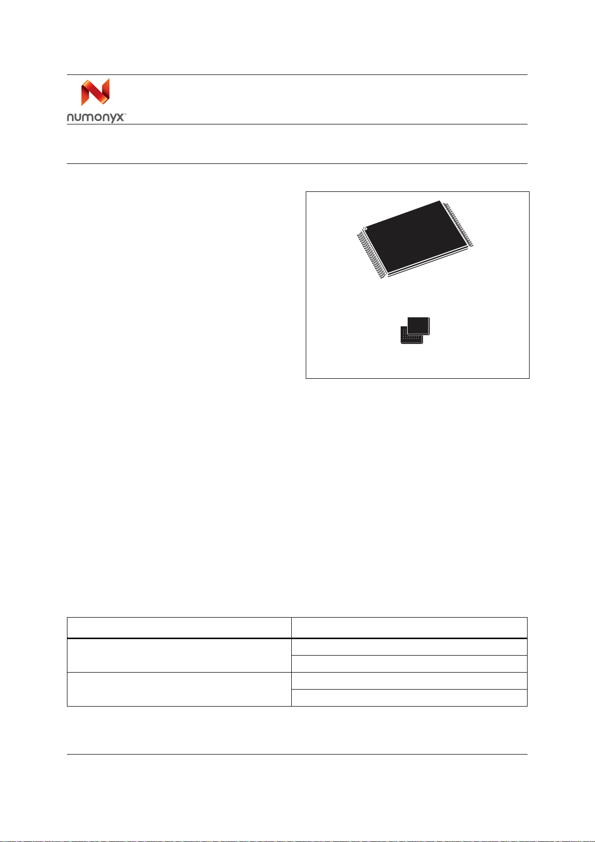
FBGA
TSOP48 12 x 20 mm
VFBGA63 9.5 x 12 x 1 mm
VFBGA63 9 x 11 x 1 mm
Table 1. Device summary
Reference Part number
NAND01G-B2B
NAND01GR3B2B, NAND01GW3B2B
NAND01GR4B2B, NAND01GW4B2B
(1)
NAND02G-B2C
NAND02GR3B2C, NAND02GW3B2C
NAND02GR4B2C, NAND02GW4B2C
(1)
1. x16 organization only available for MCP products.
www.numonyx.com
器件 Datasheet 文档搜索
AiEMA 数据库涵盖高达 72,405,303 个元件的数据手册,每天更新 5,000 多个 PDF 文件
