Datasheet 搜索 > 射频接收器 > Nordic Semiconductor > NRF24L01P-R 数据手册 > NRF24L01P-R 产品样片图册 6/197 页
 器件3D模型
¥ 7.574
NRF24L01P-R 产品样片图册 - Nordic Semiconductor
制造商:
Nordic Semiconductor
分类:
射频接收器
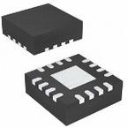
封装:
QFN-20
描述:
NRF24L01P-R 编带
Pictures:
3D模型
符号图
焊盘图
引脚图
产品图
页面导航:
引脚图在P14P15P69P115P136P137P138Hot
典型应用电路图在P12
原理图在P13P17P55P70P86P99P103P105P117P120P121P124
封装尺寸在P186
型号编码规则在P194P195
标记信息在P194
功能描述在P1P11P17P56P71P87P95P100P103P110P117P121
技术参数、封装参数在P176
应用领域在P1
电气规格在P178P182
导航目录
NRF24L01P-R数据手册
Page:
of 197 Go
若手册格式错乱,请下载阅览PDF原文件

Revision 1.6 6 of 196
nRF24LE1 Product Specification
8.5.2 Functional description of SFR registers ..........................................95
9 Interrupts .................................................................................................. 99
9.1 Features .............................................................................................. 99
9.2 Block diagram .....................................................................................99
9.3 Functional description .......................................................................... 100
9.4 SFR registers ....................................................................................... 100
9.4.1 Interrupt Enable 0 Register – IEN0.................................................. 101
9.4.2 Interrupt Enable 1 Register – IEN1 ................................................. 101
9.4.3 Interrupt Priority Registers – IP0, IP1 .............................................. 101
9.4.4 Interrupt Request Control Registers – IRCON ................................ 102
10 Watchdog................................................................................................... 103
10.1 Features ............................................................................................... 103
10.2 Block diagram ...................................................................................... 103
10.3 Functional description .......................................................................... 103
11 Power and clock management................................................................. 105
11.1 Block diagram ...................................................................................... 105
11.2 Modes of operation .............................................................................. 105
11.3 Functional description .......................................................................... 110
11.3.1 Clock control.................................................................................... 110
11.3.2 Power down control – PWRDWN .................................................... 113
11.3.3 Operational mode control - OPMCON............................................. 114
11.3.4 Reset result – RSTREAS ................................................................ 114
11.3.5 Wakeup configuration register – WUCON....................................... 115
11.3.6 Pin wakeup configuration ................................................................ 115
12 Power supply supervisor ......................................................................... 117
12.1 Features ............................................................................................... 117
12.2 Block diagram ...................................................................................... 117
12.3 Functional description .......................................................................... 117
12.3.1 Power-on reset ................................................................................ 117
12.3.2 Brown-out reset ............................................................................... 118
12.3.3 Power-fail comparator ..................................................................... 118
12.4 SFR registers ....................................................................................... 119
13 On-chip oscillators.................................................................................... 120
13.1 Features ............................................................................................... 120
13.2 Block diagrams..................................................................................... 120
13.3 Functional description .......................................................................... 121
13.3.1 16 MHz crystal oscillator.................................................................. 121
13.3.2 16 MHz RC oscillator....................................................................... 122
13.3.3 External 16 MHz clock..................................................................... 122
13.3.4 32.768 kHz crystal oscillator............................................................ 122
13.3.5 32.768 kHz RC oscillator ................................................................. 123
13.3.6 Synthesized 32.768 kHz clock......................................................... 123
13.3.7 External 32.768 kHz clock ............................................................... 123
14 MDU – Multiply Divide Unit....................................................................... 124
14.1 Features ............................................................................................... 124
14.2 Block diagram ...................................................................................... 124
器件 Datasheet 文档搜索
AiEMA 数据库涵盖高达 72,405,303 个元件的数据手册,每天更新 5,000 多个 PDF 文件
