Datasheet 搜索 > 接口芯片 > NXP(恩智浦) > PCA9615DPJ 数据手册 > PCA9615DPJ 其他数据使用手册 1/29 页
 器件3D模型
¥ 20.046
PCA9615DPJ 其他数据使用手册 - NXP(恩智浦)
制造商:
NXP(恩智浦)
分类:
接口芯片
封装:
TSSOP-10
描述:
总线缓冲器, 2通道, SMBus/I2C, 快速模式Plus, PCA9615,2.3 V至5.5 V, TSSOP-10
Pictures:
3D模型
符号图
焊盘图
引脚图
产品图
页面导航:
导航目录
PCA9615DPJ数据手册
Page:
of 29 Go
若手册格式错乱,请下载阅览PDF原文件

1. General description
The PCA9615 is a Fast-mode Plus (Fm+) SMBus/I
2
C-bus buffer that extends the normal
single-ended SMBus/I
2
C-bus through electrically noisy environments using a differential
SMBus/I
2
C-bus (dI
2
C) physical layer, which is transparent to the SMBus/I
2
C-bus protocol
layer. It consists of two single-ended to differential driver channels for the SCL (serial
clock) and SDA (serial data).
The use of differential transmission lines between identical dI
2
C bus buffers removes
electrical noise and common-mode offsets that are present when signal lines must pass
between different voltage domains, are bundled with hostile signals, or run adjacent to
electrical noise sources, such as high energy power supplies and electric motors.
The SMBus/I
2
C-bus was conceived as a simple slow speed digital link for short runs,
typically on a single PCB or between adjacent PCBs with a common ground connection.
Applications that extend the bus length or run long cables require careful design to
preserve noise margin and reject interference.
The dI
2
C-bus buffers were designed to solve these problems and are ideally suited for
rugged high noise environments and/or longer cable applications, allow multiple slaves,
and operate at bus speeds up to 1 MHz clock rate. Cables can be extended to at least
3 meters (3 m), or longer cable runs at lower clock speeds. The dI
2
C-bus buffers are
compatible with existing SMBus/I
2
C-bus devices and can drive Standard, Fast-mode, and
Fast-mode Plus devices on the single-ended side.
Signal direction is automatic, and requires no external control. To prevent bus latch up,
the standard SMBus/I
2
C-bus side of the bus buffer, the PCA9615 employs static offset,
care should be taken when connecting these to other SMBus/I
2
C-bus buffers that may not
operate with offset.
This device is a bridge between the normal 2-wire single-ended wired-OR SMBus/I
2
C-bus
and the 4-wire dI
2
C-bus.
Additional circuitry allows the PCA9615 to be used for ‘hot swap’ applications, where
systems are always on, but require insertion or removal of modules or cards without
disruption to existing signals.
The PCA9615 has two supply voltages, V
DD(A)
and V
DD(B)
. V
DD(A)
, the card side supply,
only serves as a reference and ranges from 2.3 V to 5.5 V. V
DD(B)
, the line side supply,
serves as the majority supply for circuitry and ranges from 3.0 V to 5.5 V.
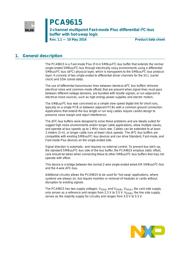
PCA9615
2-channel multipoint Fast-mode Plus differential I
2
C-bus
buffer with hot-swap logic
Rev. 1.1 — 10 May 2016 Product data sheet
器件 Datasheet 文档搜索
AiEMA 数据库涵盖高达 72,405,303 个元件的数据手册,每天更新 5,000 多个 PDF 文件
