Datasheet 搜索 > 微控制器 > Microchip(微芯) > PIC16F1503-E/ST 数据手册 > PIC16F1503-E/ST 其他数据使用手册 1/26 页
 器件3D模型
¥ 7.832
PIC16F1503-E/ST 其他数据使用手册 - Microchip(微芯)
制造商:
Microchip(微芯)
分类:
微控制器
封装:
TSSOP-14
描述:
PIC16F1503 8 位闪存微控制器Microchip 的 PIC16F 系列微控制器 8 位 MCU,将 Microchip 的 PIC® 体系架构融入到引脚和封装选件中,从节省空间的 14 引脚设备到功能丰富的 64 引脚设备。 带有基线、中级或增强型中级体系架构的设备提供多种不同的外围设备组合,可谓设计人员提供灵活性,并为应用提供选择。 PIC16F1503 系列微控制器基于 Microchip 的增强型中级内核,带 16 层深硬件堆栈和 49 个指令。 这些 MCU 可提供高达 5 MIP、3.5 千字节的程序存储器,数据存储器为 128 字节 RAM。 板载可配置振荡器,精确度为 ±1%。### 微控制器功能最大 20 MHz CPU 速度 49 个指令 16 级硬件堆栈 16 MHz 内部振荡器 - 可选频率范围 16 MHz 至 32 kHz 12 个输入/输出引脚 通电重置 (POR) 通电计时器 (PWRT) 可编程低功率掉电重置 (LPBOR) 延长监控计时器 (WDT) 在线串行编程 (ICSP) 在线调试 (ICD) ### 外设8 通道 10 位模拟到数字转换器 (ADC) 数字到模拟转换器 (DAC) 两个比较器 电压参考 两个 8 位计时器 一个 16 位计时器 四个 10 位 PWM 模块 主同步串行端口 (MSSP),带有 SPI 和 I2C 两个可配置逻辑单元 (CLC) 模块 互补波形发生器 (CWG) ### PIC16 微控制器展开
Pictures:
3D模型
符号图
焊盘图
引脚图
产品图
页面导航:
原理图在P14P22
导航目录
PIC16F1503-E/ST数据手册
Page:
of 26 Go
若手册格式错乱,请下载阅览PDF原文件

2012 Microchip Technology Inc. DS41631B-page 1
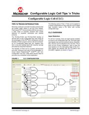
Configurable Logic Cell Tips ’n Tricks
TIPS ‘N TRICKS INTRODUCTION
Microchip continues to provide innovative products that
are smaller, faster, easier to use and more reliable.
Flash-based PIC
®
microcontrollers (MCUs) are used in
a wide range of everyday products from smoke
detectors to industrial, automotive and medical
products.
The PIC16(L)F150X and PIC10(L)F32X families of
devices with on-chip configurable logic cells merge all
the advantages of the PIC
®
MCU architecture and the
flexibility of Flash program memory with the functional-
ity of a configurable digital logic cell. Together, they
form a low-cost building block with resource savings
and external component reduction.
The flexibility of Flash and an excellent development
tool suite, including a low-cost In-Circuit Debugger, In-
Circuit Serial Programming
TM
(ICSP
TM
) and CLC
Configuration Tool GUI, make these devices ideal for
just about any embedded control application.
The following series of Tips ‘n Tricks can be applied to
a variety of applications to help make the most of digital
logic functions using a PIC MCU with on-chip
configurable logic.
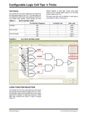
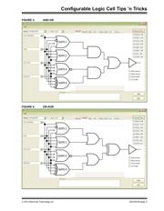
CLC OVERVIEW
Input Selection
For all CLC modules, there are eight signals available
as inputs to the configurable logic cell, and these eight
input signals may vary from device to device. Neverthe-
less, only four can be selected at any one time. This is
done via four 8-input multiplexers, used to pass the
input signals on to the data gating stage of the CLC.
Input signals are selected with the CLCxSEL0 and
CLCxSEL1 registers, as shown in Figure 1.
FIGURE 1: CLC CONFIGURATION
Configurable Logic Cell (CLC)
器件 Datasheet 文档搜索
AiEMA 数据库涵盖高达 72,405,303 个元件的数据手册,每天更新 5,000 多个 PDF 文件
