Datasheet 搜索 > 微控制器 > Microchip(微芯) > PIC16F1936-E/SS 数据手册 > PIC16F1936-E/SS 其他数据使用手册 1/40 页
 器件3D模型
¥ 16.722
PIC16F1936-E/SS 其他数据使用手册 - Microchip(微芯)
制造商:
Microchip(微芯)
分类:
微控制器
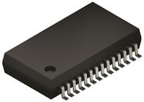
封装:
SSOP-28
描述:
PIC16F1934/1936/1937 8 位闪存微控制器Microchip 的 PIC16F 系列微控制器 8 位 MCU,将 Microchip 的 PIC® 体系架构融入到引脚和封装选件中,从节省空间的 14 引脚设备到功能丰富的 64 引脚设备。 带有基线、中级或增强型中级体系架构的设备提供多种不同的外围设备组合,可谓设计人员提供灵活性,并为应用提供选择。 PIC16F1934/1936/1937 系列微控制器基于 Microchip 的增强型中级内核,带 16 层深硬件堆栈和 49 个指令。 这些 MCU 提供高达 8 个 MIP、14 千字节程序存储器、512 字节 RAM 和 256 字节数据 EEPROM。 板载可配置振荡器,精确度为 ±1%。### 微控制器功能最大 32 MHz CPU 速度 49 个指令 16 级硬件堆栈 32 MHz 内部振荡器 - 可选频率范围 32 MHz 至 31 kHz 36 个输入/输出引脚 –PIC16F1934/1937 25 个输入/输出引脚 –PIC16F1936 nanoWatt XLP 技术 通电重置 (POR) 通电计时器 (PWRT) 振荡器启动计时器 (OST) 掉电重置 (BOR) 监控器计时器 (WDT) 低电压编程 (LVP) 在线串行编程 (ICSP) 在线调试 (ICD) ### 外设集成 LCD 控制器 - PIC16F1936 60 段、PIC16F1934/1937 96 段 10 位模拟至数字转换器 (ADC) - PIC16F1936 11 通道、PIC16F1934/1937 14 通道 mTouchTM 电容性传感器模块 - PIC16F1936 8 通道、PIC16F1934/1937 16 通道 两个捕获/比较/PWM (CCP) 模块 - 仅限 PIC16F1827 三个增强型捕获/比较/PWM (ECCP) 模块 两个比较器 四个 8 位计时器 一个 16 位计时器 主同步串行端口 (MSSP),带有 SPI 和 I2C 增强型通用同步异步接收器发射器 (EUSART) 固定电压参考 (FVR) SR 闩锁 ### PIC16 微控制器展开
Pictures:
3D模型
符号图
焊盘图
引脚图
产品图
页面导航:
引脚图在P1Hot
技术参数、封装参数在P33
电气规格在P33
导航目录
PIC16F1936-E/SS数据手册
Page:
of 40 Go
若手册格式错乱,请下载阅览PDF原文件
© 2008 Microchip Technology Inc. Advance Information DS41360A-page 1
PIC16F193X/LF193X
This document includes the
programming specifications for the
following devices:
1.0 OVERVIEW
The PIC16F193X and PIC16LF193X devices can be
programmed using either the high-voltage In-Circuit
Serial Programming™ (ICSP™) method or the
low-voltage ICSP™ method.
1.1 Hardware Requirements
1.1.1 HIGH-VOLTAGE ICSP
PROGRAMMING
In High-Voltage ICSP™ mode, the PIC16F193X and
PIC16LF193X devices require two programmable
power supplies: one for V
DD and one for the
MCLR
/VPP/RE3 pin.
1.1.2 LOW-VOLTAGE ICSP
PROGRAMMING
In Low-Voltage ICSP™ mode, the PIC16F193X and
PIC16LF193X devices can be programmed using a
single V
DD source in the operating range. The
MCLR
/VPP/RE3 pin does not have to be brought to a
different voltage, but can instead be left at the normal
operating voltage.
1.1.2.1 Single-Supply ICSP Programming
The LVP bit in Configuration Word 2 enables
single-supply (low-voltage) ICSP programming. The
LVP bit defaults to a ‘1’ (enabled) from the factory. The
LVP bit may only be programmed to ‘0’ by entering the
High-Voltage ICSP mode, where MCLR/VPP/RE3 pin is
raised to V
IHH. Once the LVP bit is programmed to a ‘0’,
only the High-Voltage ICSP mode is available and only
the High-Voltage ICSP mode can be used to program
the device.
1.2 Pin Utilization
Five pins are needed for ICSP™ programming. The
pins are listed in Table 1-1.
TABLE 1-1: PIN DESCRIPTIONS DURING PROGRAMMING
• PIC16F1933 • PIC16F1934 • PIC16F1936
• PIC16F1937 • PIC16F1938 • PIC16F1939
• PIC16LF1933 • PIC16LF1934 • PIC16LF1936
• PIC16LF1937 • PIC16LF1938 • PIC16LF1939
Note 1: The High-Voltage ICSP mode is always
available, regardless of the state of the
LVP bit, by applying VIHH to the
MCLR
/VPP/RE3 pin.
2: While in Low-Voltage ICSP mode, MCLR
is always enabled, regardless of the
MCLRE bit, and RE3 pin can no longer be
used as a general purpose input.
Pin Name
During Programming
Function Pin Type Pin Description
RB6 ICSPCLK I Clock Input – Schmitt Trigger Input
RB7 ICSPDAT I/O Data Input/Output – Schmitt Trigger Input
RE3/MCLR
/VPP Program/Verify mode P
(1)
Program Mode Select/Programming Power Supply
V
DD VDD P Power Supply
V
SS VSS P Ground
Legend: I = Input, O = Output, P = Power
Note 1: In the PIC16F193X/LF193X, the programming high voltage is internally generated. To activate the Program/Verify
mode, high voltage needs to be applied to MCLR
input. Since the MCLR is used for a level source, MCLR does not
draw any significant current.
PIC16F193X/LF193X Memory Programming Specification
器件 Datasheet 文档搜索
AiEMA 数据库涵盖高达 72,405,303 个元件的数据手册,每天更新 5,000 多个 PDF 文件
