Datasheet 搜索 > 微控制器 > Microchip(微芯) > PIC16F1947-E/MR 数据手册 > PIC16F1947-E/MR 其他数据使用手册 5/13 页
 器件3D模型
¥ 19.68
PIC16F1947-E/MR 其他数据使用手册 - Microchip(微芯)
制造商:
Microchip(微芯)
分类:
微控制器
封装:
QFN-64
描述:
8位微控制器 -MCU 28KB1KB RAM 256B EEPROM
Pictures:
3D模型
符号图
焊盘图
引脚图
产品图


PIC16F1947-E/MR数据手册
Page:
of 13 Go
若手册格式错乱,请下载阅览PDF原文件

2010-2014 Microchip Technology Inc. DS80000497G-page 5
PIC16(L)F1946/1947
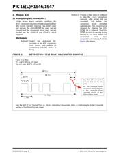
In Figure 1, 88 instruction cycles (TCY) will be
required to complete the full conversion. Each T
AD
cycle consists of eight TCY periods. A fixed delay is
provided to stop the A/D conversion after 86
instruction cycles and terminate the conversion at
the correct time as shown in the figure above.
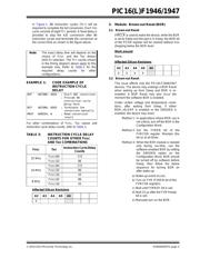
EXAMPLE 1: CODE EXAMPLE OF
INSTRUCTION CYCLE
DELAY
For other combinations of FOSC, TAD values and
Instruction cycle delay counts, refer to Tabl e 3.
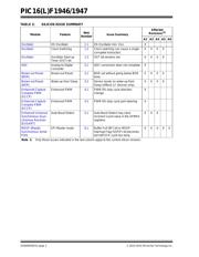
TABLE 3: INSTRUCTION CYCLE DELAY
COUNTS FOR OTHER F
OSC
AND T
AD COMBINATIONS
Affected Silicon Revisions
3. Module: Brown-out Reset (BOR)
3.1 Brown-out Reset
If MCLR
is used to wake the device, while the BOR
is set to Sleep and the part is in Sleep, the BOR bit
of the PCON register will be cleared without VDD
dropping below the BOR level.
Work around
None.
Affected Silicon Revisions
3.2 Brown-out Reset
This issue affects only the PIC16LF1946/1947
devices. The device may undergo a BOR Reset
when waking up from Sleep and BOR is re-
enabled. A BOR Reset may also occur the
moment the software BOR is enabled.
Under certain voltage and temperature condi-
tions, after waking from Sleep, if either
BOR_nSLEEP is enabled or the SBODEN is
enabled, the device may reset.
Method 1: In applications where BOR use is
not critical, turn off the BOR in the
Configuration Word.
Method 2: Set the FVREN bit of the
FVRCON register. Maintain this
bit on at all times.
Method 3: When the BOR module is needed
only during run-time, use the
software-enabled BOR by setting
the SBODEN option on the
Configuration Word. BOR should
be turned off by software before
Sleep, then follow the below
sequence for turning BOR on
after wake-up:
a) Wake-up event occurs;
b) Turn on FVR (FVREN bit of the
FVRCON register);
c) Wait until FVRRDY bit is set;
d) Wait 15 µs after the FVR Ready
bit is set;
e) Manually turn on the BOR.
Note: The exact delay time will depend on the
choice of F
OSC and the TAD divisor
(ADCS) selection. The T
CY counts shown
in the timing diagram above apply to this
example only. Refer to Table 3 for the
required delay counts for other
configurations.
F
OSC TAD
Instruction Cycle Delay
Counts
32 MHz
F
OSC/64 172
FOSC/32 86
16 MHz
F
OSC/64 172
F
OSC/32 86
F
OSC/16 43
8 MHz
FOSC/32 86
F
OSC/16 43
A2 A3 A4 A5 A6
X
BSF ADCON0, ADGO ; Start ADC conversion
; Provide 86
instruction cycle
delay here
BCF ADCON0, ADGO ; Terminate the
conversion manually
MOVF ADRESH, W ; Read conversion
result
A2 A3 A4 A5 A6
XXXX
器件 Datasheet 文档搜索
AiEMA 数据库涵盖高达 72,405,303 个元件的数据手册,每天更新 5,000 多个 PDF 文件
