Datasheet 搜索 > 微控制器 > Microchip(微芯) > PIC16F628AT-E/SO 数据手册 > PIC16F628AT-E/SO 产品描述及参数 4/18 页
 器件3D模型
¥ 8.161
PIC16F628AT-E/SO 产品描述及参数 - Microchip(微芯)
制造商:
Microchip(微芯)
分类:
微控制器
封装:
SOIC-18
描述:
PIC16 系列 224 B RAM 3.5 kB 闪存 8位 CMOS 微控制器 - SOIC-18
Pictures:
3D模型
符号图
焊盘图
引脚图
产品图
页面导航:
应用领域在P3
导航目录
PIC16F628AT-E/SO数据手册
Page:
of 18 Go
若手册格式错乱,请下载阅览PDF原文件

MPLAB
®
ICE 2000
DS51140N-page 4 © 2007 Microchip Technology Inc.
4.3.2 CLOCK SOURCE FROM THE TARGET
APPLICATION
If the target application is selected to provide the clock
source, the target board must also be selected to
power the emulator processor (see the MPLAB ICE
2000 on-line help file in MPLAB IDE (Help>Topics
) or
the “MPLAB
®
ICE 2000 In-Circuit Emulator User’s
Guide” (DS51488), “Using a Target Board Clock”).
At low voltage, the maximum speed of the processor
will be limited to the rated speed of the device under
emulation.
An oscillator circuit on the device adapter generates a
clock to the processor module and buffers the clock
circuit on the target board. In this way, the MPLAB ICE
2000 emulator closely matches the oscillator options of
the actual device. All oscillator modes are supported
(as documented in the device’s data sheet) except as
noted in Section 3.0 “Emulator-Related Issues”. The
OSC1 and OSC2 inputs of the device adapter have a
5 pF to 10 pF load. Be aware of this when using a
crystal in HS, XT, LP or LF modes, or an RC network in
RC mode.
The frequency of the emulated RC network may vary
relative to the actual device due to emulator circuitry.
If a specific frequency is important, adjust the RC val-
ues to achieve the desired frequency. Another alterna-
tive would be to allow the emulator to provide the
clock as described in Section 4.3.1 “Clock Source
from Emulator”.
When using the target board clock, the system’s
operating voltage is between 2.5V and 5.5V.
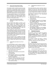
4.4 ESD Protection and Electrical
Overstress
All CMOS chips are susceptible to electrostatic
discharge (ESD). In the case of the processor modules,
the pins of the CMOS emulator are directly connected
to the target connector, making the chip vulnerable to
ESD. ESD can also induce latch-up in CMOS chips,
causing excessive current through the chip and
possible damage. MPLAB ICE 2000 has been
designed to minimize potential damage by implement-
ing overcurrent protection and transient suppressors.
However, care should be given to minimizing ESD
conditions while using the system.
During development, contention on an I/O pin is
possible (e.g., when an emulator pin is driving a ‘1’ and
the target board is driving a ‘0’). Prolonged contention
may cause latch-up and damage to the emulator chip.
One possible precaution is to use current limiting
resistors (~100 Ω) during the development phase on
bidirectional I/O pins. Using limiting resistors can also
help avoid damage to modules, device adapters and
pods that occurs when a voltage source is accidentally
connected to an I/O pin on the target board.
4.5 Freeze Mode
The MPLAB ICE 2000 system allows the option of
“freezing” peripheral operation or allowing them to
continue operating when the processor is halted. This
option is configured in the MPLAB IDE. The Freeze
function is available on all processor modules except
the PCM16XA0.
This function is useful to halt an on-board timer while at
a break point. At a break point and while single
stepping, interrupts are disabled.
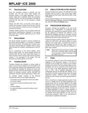
5.0 DEVICE ADAPTERS
Device adapters are identified by a DVA number (e.g.,
DVA16XP180, DVA1003). To determine which device
adapters support which processor modules, refer to the
file “Readme for MPLAB ICE 2000.txt” in the MPLAB
IDE installation directory.
Components on the device adapter are powered by the
target board, even when the emulator processor
module is being powered by the emulator system and
running an internal clock. This will cause a maximum
10 mA current draw from the target system.
5.1 Emulating a .600 28-Pin Part
When emulating a .600 wide, 28-pin device, an adapter
will be needed to convert the standard .300 wide
socket on the device adapters to the .600 wide socket
on the target board.
There are many adapters available for this purpose,
such as Digi-Key part number A502-ND.
5.2 T1OSC Jumper
Some device adapters are equipped with a 3-pin
jumper to force the device adapter to enable/disable
the Timer1 oscillator circuitry.
When in the “ON” position, the device adapter’s Timer1
oscillator circuitry is always enabled regardless of the
T1OSCEN bit in T1CON.
When in the “OFF” position, the device adapter’s
Timer1 oscillator circuit is enabled/disabled by software
in application code by the T1OSCEN bit in T1CON.
Note: PCM16XB0/B1, PCM16XE0/E1,
PCM16XK0 and PCM16XL0 do not
support software enable/disable of the
Timer1 circuitry and must use the jumper
to either enable or disable the function (see
Table 5-7 for DVA16XP282, DVA16XP401,
DVA16XL441 and DVA16PQ441).
器件 Datasheet 文档搜索
AiEMA 数据库涵盖高达 72,405,303 个元件的数据手册,每天更新 5,000 多个 PDF 文件
