Datasheet 搜索 > 微控制器 > Microchip(微芯) > PIC16F74-I/P 数据手册 > PIC16F74-I/P 产品描述及参数 5/18 页
 器件3D模型
¥ 35.674
PIC16F74-I/P 产品描述及参数 - Microchip(微芯)
制造商:
Microchip(微芯)
分类:
微控制器
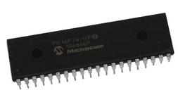
封装:
DIP-40
描述:
PIC16F73/74/76/77 8 位闪存微控制器Microchip 的 PIC16F 系列微控制器 8 位 MCU,将 Microchip 的 PIC® 体系架构融入到引脚和封装选件中,从节省空间的 14 引脚设备到功能丰富的 64 引脚设备。 带有基线、中级或增强型中级体系架构的设备提供多种不同的外围设备组合,可谓设计人员提供灵活性,并为应用提供选择。 PIC16F73/74/76/77 系列微控制器基于 Microchip 的中级内核,带 8 层深硬件堆栈和 35 个指令。 这些 MCU 提供高达 5 个 MIP、14 千字节程序存储器和 368 字节 RAM。### 微控制器功能最大 20 MHz CPU 速度 35 指令 8 级硬件堆栈 22 个输入/输出引脚 – PIC16F73/76 型号 33 个输入/输出引脚 – PIC16F74/77 型号 通电重置 (POR) 通电计时器 (PWRT) 振荡器启动计时器 (OST) 掉电重置 (BOR) 监控器计时器 (WDT) 在线串行编程 (ICSP) 在线调试 (ICD) ### 外设8 位模拟到数字转换器 (ADC) - PIC16F73/76 5 通道、PIC16F74/77 8 通道 两个捕获、比较、PWM (CCP) 模块 两个 8 位计时器 一个 16 位计时器 同步串行端口 (SSP),带有 SPI 和 I2C 通用同步异步接收器发射器 (USART) ### PIC16 微控制器展开
Pictures:
3D模型
符号图
焊盘图
引脚图
产品图
页面导航:
应用领域在P3
导航目录
PIC16F74-I/P数据手册
Page:
of 18 Go
若手册格式错乱,请下载阅览PDF原文件
© 2007 Microchip Technology Inc. DS51140N-page 5
5.3 Power and Ground Detection
Two test points are provided on some device adapters
for the following: GND (black) and VCCME (red).
On certain Device Adapters, to visually indicate Target
Power mode, the “target power” LED will illuminate”
5.4 Specific Device Adapter Issues
This section details processor-specific considerations
that have been made on device adapters. Only
adapters with special considerations are listed.
5.4.1 DVA12XP080
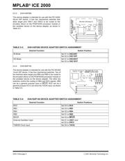
5.4.2 DVA12XP081
This device adapter is intended for use with PIC12C50X
8-pin DIP devices. It has four mechanical switches that
allow target pins GP2 to GP5 to be routed to the emulator
silicon on the PCM16XA0 processor module or the
oscillator chip on the device adapter, as shown in Table 5-1.
In addition, a 24C00 EEPROM (U1) is connected to
RA0 and RA1 of the emulator silicon to support the
EEPROM capabilities of the PIC12CE51X family devices.
For information on how to use EEPROM memory, see the
MPLAB IDE on-line device-specific limitations for the
PCM16XA0 (PIC12CE518/519) devices by selecting
Debugger>Settings
, clicking the Limitations tab, and then
clicking the Details button.
TABLE 5-1: DVA12XP080 DEVICE ADAPTER SWITCH ASSIGNMENT
Desired Function Switch Positions
RB2 Set S4 to RB2
RB3 Set S3 to RB3
RB4 Set S2 to RB4
RB5 Set S1 to RB5
MCLR
Set S3 to MCLR
External Oscillator Input Set S1 to OSC1 and
set S2 to OSC2
TIMER0 Clock Input Set S4 to T0CKI
This device adapter is intended for use with PIC12C67X
8-pin DIP devices. It has two mechanical switches that
allow target pins GP4 and GP5 to be routed to the emulator
silicon on the PCM12XA0 processor module or the
oscillator device on the device adapter, as shown in
Table 5-2.
TABLE 5-2: DVA12XP081 DEVICE ADAPTER SWITCH ASSIGNMENT
Desired Function Switch Positions
GP4 Set S2 to GP4
GP5 Set S1 to GP5
External Oscillator Input Set S1 to OSC1 and
set S2 to OSC2
器件 Datasheet 文档搜索
AiEMA 数据库涵盖高达 72,405,303 个元件的数据手册,每天更新 5,000 多个 PDF 文件
