Datasheet 搜索 > 微控制器 > Microchip(微芯) > PIC18F46K20-E/P 数据手册 > PIC18F46K20-E/P 其他数据使用手册 6/12 页
 器件3D模型
¥ 27.833
PIC18F46K20-E/P 其他数据使用手册 - Microchip(微芯)
制造商:
Microchip(微芯)
分类:
微控制器
封装:
PDIP-40
描述:
PIC18 系列 3936 B RAM 64 kB 闪存 8位 微控制器 - PDIP-40
Pictures:
3D模型
符号图
焊盘图
引脚图
产品图
页面导航:
封装信息在P9
导航目录
PIC18F46K20-E/P数据手册
Page:
of 12 Go
若手册格式错乱,请下载阅览PDF原文件
PIC18F26K20/46K20
DS80000379C-page 6 2008-2015 Microchip Technology Inc.
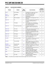
15. Module: System Clocks
HFINTOSC output frequency is 16 MHz ± 3%,
25°C to 85°C.
Work around
None.
Affected Silicon Revisions
16. Module: POR/BOR
The POR rearm voltage may be below the low end
of the BOR range causing unexpected code
execution below the BOR range.
Work around
Use external power monitor to hold device in
Reset below 1.1 Volts.
Affected Silicon Revisions
17. Module: POR
The POR may release around 0.8 volts (below the
POR rearm voltage of 1.2V nominal) when V
DD
rises from below either 0.60V when BOR is not
enabled, or 0.33V when BOR is enabled.
Work around
Use Power-up Timer when operating with the EC,
EXTRC or HFINTOSC oscillator modes. Ensure
that V
DD rise time is less than the Power-up Timer
time.
Affected Silicon Revisions
18. Module: POR
The part may hang in the Reset state when VDD
falls to the POR rearm threshold of approximately
1.2 volts then rises at a rate faster than 7500 volts
per second to the operating range. Recovery from
the hung state is possible only by first lowering
V
DD to below the POR rearm threshold followed by
raising V
DD to the operating range.
Work around
Slow VDD rise time by adding series resistance
between the voltage supply and the V
DD pin. VDD
bypassing should remain on the pin side of the
series resistor.
Affected Silicon Revisions
19. Module: Clocks
EC Mode operation is limited to a maximum of
48 MHz.
Work around
Use HS Clock mode for external clocking above
48 MHz.
Affected Silicon Revisions
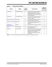
20. Module: Comparators
Comparator input offset voltage is ± 25 mV and
may degrade over the lifetime of the part
accelerated by high temperature. The offset voltage
increases as the common-mode voltage decreases
with the following characteristics: Offset is ± 25 mV
when the common-mode voltage is V
DD; The offset
is up to ± 50 mV when the common-mode voltage
is VDD/2; The offset is greater than ± 50 mV when
the common-mode voltage is 0V.
Work around
None.
Affected Silicon Revisions
21. Module: Comparators
When the CxON bit is clear, the output from the
comparator will be properly forced to zero, but the
CxPOL bit will improperly have no effect on the
CxOUT bit. This prevents presetting the compara-
tor change-on-interrupt mismatch latches as
described in the data sheet.
Work around
Configure one of the unused comparator input
channels as a digital output. Use that digital output
to manipulate the comparator output to the desired
CxOUT non-interrupt level. When the comparator
A4
A5
X
X
A4 A5
X
X
A4
A5
X
X
A4 A5
X
X
A4
A5
X
X
A4 A5
X
X
器件 Datasheet 文档搜索
AiEMA 数据库涵盖高达 72,405,303 个元件的数据手册,每天更新 5,000 多个 PDF 文件
