Datasheet 搜索 > 微控制器 > Microchip(微芯) > PIC24FJ256GA106-I/PT 数据手册 > PIC24FJ256GA106-I/PT 其他数据使用手册 1/332 页
 器件3D模型
¥ 48.89
PIC24FJ256GA106-I/PT 其他数据使用手册 - Microchip(微芯)
制造商:
Microchip(微芯)
分类:
微控制器
封装:
TQFP-64
描述:
PIC24FJxxxGA106/108/110 16 位闪存微控制器### PIC24 微控制器
Pictures:
3D模型
符号图
焊盘图
引脚图
产品图
页面导航:
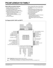
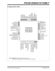
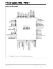
引脚图在P15P16P17P18P19P20P21P22P24P187P228P233Hot
典型应用电路图在P243P244
原理图在P14P30P67P129P157P160P161P165P170P172P177P178
封装尺寸在P307
标记信息在P305
封装信息在P270P305P307P308P309P310P311P312P314P318P329
功能描述在P165P169P203P213
技术参数、封装参数在P187P271P278P279P280P281P282P283P285P286P287P290
电气规格在P25P70P255P320

导航目录
PIC24FJ256GA106-I/PT数据手册
Page:
of 332 Go
若手册格式错乱,请下载阅览PDF原文件
2007-2019 Microchip Technology Inc. DS30009905F-page 1
PIC24FJ256GA110 FAMILY
Power Management:
• On-Chip 2.5V Voltage Regulator
• Switch between Clock Sources in Real Time
• Idle, Sleep and Doze modes with Fast Wake-up and
Two-Speed Start-up
• Run mode: 1 mA/MIPS, 2.0V Typical
• Standby Current with 32 kHz Oscillator: 2.6 A,
2.0V Typical
High-Performance CPU:
• Modified Harvard Architecture
• Up to 16 MIPS Operation at 32 MHz
• 8 MHz Internal Oscillator
• 17-Bit x 17-Bit Single-Cycle Hardware Multiplier
• 32-Bit by 16-Bit Hardware Divider
• 16 x 16-Bit Working Register Array
• C Compiler Optimized Instruction Set Architecture with
Flexible Addressing modes
• Linear Program Memory Addressing, Up to 12 Mbytes
• Linear Data Memory Addressing, Up to 64 Kbytes
• Two Address Generation Units (AGUs) for Separate
Read and Write Addressing of Data Memory
Analog Features:
• 10-Bit, Up to 16-Channel Analog-to-Digital (A/D)
Converter at 500 ksps:
- Conversions available in Sleep mode
• Three Analog Comparators with Programmable Input/
Output Configuration
• Charge Time Measurement Unit (CTMU)
Peripheral Features:
• Peripheral Pin Select:
- Allows independent I/O mapping of many
peripherals at run time
- Continuous hardware integrity checking and safety
interlocks prevent unintentional configuration changes
- Up to 46 available pins (100-pin devices)
• Three 3-Wire/4-Wire SPI modules (support
4 Frame modes) with 8-Level FIFO Buffer
• Three I
2
C modules support Multi-Master/Slave modes
and 7-Bit/10-Bit Addressing
• Four UART modules:
- Supports RS-485, RS-232, LIN/J2602 protocols
and IrDA
®
- On-chip hardware encoder/decoder for IrDA
- Auto-wake-up and Auto-Baud Detect (ABD)
- 4-level deep FIFO buffer
• Five 16-Bit Timers/Counters with Programmable Prescaler
• Nine 16-Bit Capture Inputs, each with a
Dedicated Time Base
• Nine 16-Bit Compare/PWM Outputs, each with a
Dedicated Time Base
• 8-Bit Parallel Master Port (PMP/PSP):
- Up to 16 address pins
- Programmable polarity on control lines
• Hardware Real-Time Clock/Calendar (RTCC):
- Provides clock, calendar and alarm functions
• Programmable Cyclic Redundancy Check (CRC) Generator
• Up to Five External Interrupt Sources
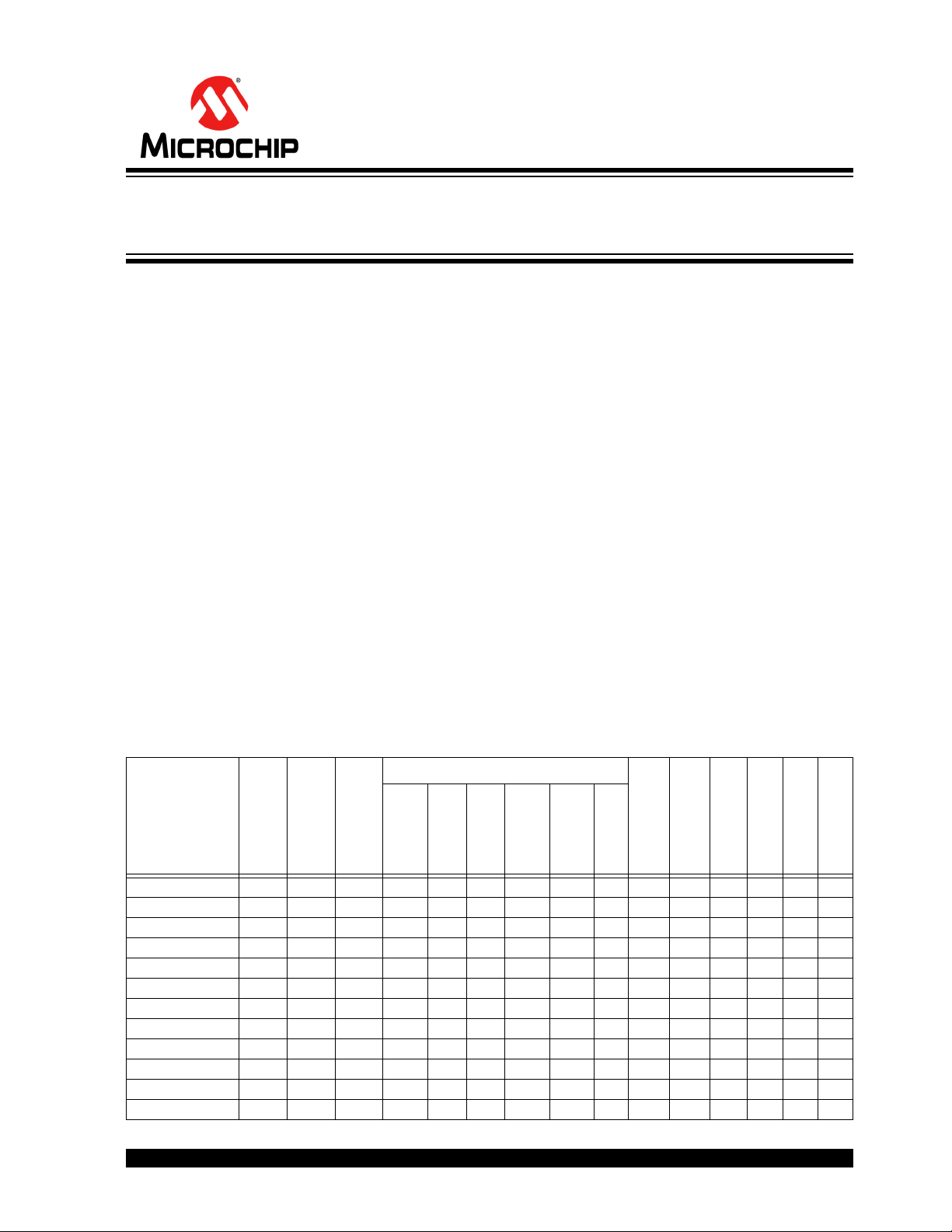
Devices
Pins
Program
Memory (Bytes)
SRAM (Bytes)
Remappable Peripherals
I
2
C
10-Bit A/D (ch)
Comparators
PMP/PSP
JTAG
CTMU
Remappable
Pins
Timers 16-Bit
Capture Input
Compare/
PWM Output
UART w/ IrDA
®
SPI
PIC24FJ64GA106 64 64K 16K 31 5 9 9 4 3 3 16 3 Y Y Y
PIC24FJ128GA106 64 128K 16K 31 5 9 9 4 3 3 16 3 Y Y Y
PIC24FJ192GA106 64 192K 16K 31 5 9 9 4 3 3 16 3 Y Y Y
PIC24FJ256GA106 64 256K 16K 31 5 9 9 4 3 3 16 3 Y Y Y
PIC24FJ64GA108 80 64K 16K 42 5 9 9 4 3 3 16 3 Y Y Y
PIC24FJ128GA108 80 128K 16K 42 5 9 9 4 3 3 16 3 Y Y Y
PIC24FJ192GA108 80 192K 16K 42 5 9 9 4 3 3 16 3 Y Y Y
PIC24FJ256GA108 80 256K 16K 42 5 9 9 4 3 3 16 3 Y Y Y
PIC24FJ64GA110 100 64K 16K 46 5 9 9 4 3 3 16 3 Y Y Y
PIC24FJ128GA110 100 128K 16K 46 5 9 9 4 3 3 16 3 Y Y Y
PIC24FJ192GA110 100 192K 16K 46 5 9 9 4 3 3 16 3 Y Y Y
PIC24FJ256GA110 100 256K 16K 46 5 9 9 4 3 3 16 3 Y Y Y
64/80/100-Pin, 16-Bit, General Purpose
Flash Microcontrollers with Peripheral Pin Select (PPS)
器件 Datasheet 文档搜索
AiEMA 数据库涵盖高达 72,405,303 个元件的数据手册,每天更新 5,000 多个 PDF 文件
