Datasheet 搜索 > 16位微控制器 > Microchip(微芯) > PIC24FJ256GA406-I/MR 数据手册 > PIC24FJ256GA406-I/MR 其他数据使用手册 1/554 页
 器件3D模型
¥ 44.2
PIC24FJ256GA406-I/MR 其他数据使用手册 - Microchip(微芯)
制造商:
Microchip(微芯)
分类:
16位微控制器
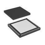
封装:
QFN-64
描述:
MICROCHIP PIC24FJ256GA406-I/MR 微控制器, 16位, 通用, PIC24FJ, 32 MHz, 256 KB, 16 KB, 64 引脚, QFN
Pictures:
3D模型
符号图
焊盘图
引脚图
产品图
页面导航:
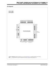
引脚图在P3P4P5P6P7P8P9P10P11P12P13P14Hot
典型应用电路图在P454P455
原理图在P25P26P58P89P101P187P209P243P248P249P253P256
封装尺寸在P527
标记信息在P525P526
封装信息在P496P525P527P528P529P530P531P532P534P535P536P551
功能描述在P4P6P8P10P12P13P15P16P269P275P357P387
技术参数、封装参数在P301P497P501P502P503P504P505P506P508P522P523P524
应用领域在P1P102P103P195
电气规格在P53P210P462P479


导航目录
PIC24FJ256GA406-I/MR数据手册
Page:
of 554 Go
若手册格式错乱,请下载阅览PDF原文件

2015 Microchip Technology Inc. DS30010089C-page 1
PIC24FJ256GA412/GB412 FAMILY
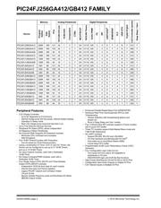
Extreme Low-Power Features
• Multiple Power Management Options for Extreme Power
Reduction:
-V
BAT
allows for lowest power consumption on backup
battery (with or without RTCC)
- Deep Sleep allows near total power-down with the ability to
wake-up on external triggers
- Sleep and Idle modes selectively shut down peripherals
and/or core for substantial power reduction and fast wake-up
- Doze mode allows CPU to run at a lower clock speed than
peripherals
• Alternate Clock modes allow On-the-Fly Switching to a Lower
Clock Speed for Selective Power Reduction
• Extreme Low-Power Current Consumption for Deep Sleep:
- WDT: 650 nA @ 2V typical
- RTCC: 650 nA @ 32 kHz, 2V typical
- Deep Sleep current, 60 nA typical
• 160 A/MHz in Run mode
High-Performance CPU
• Modified Harvard Architecture
• Up to 16 MIPS Operation @ 32 MHz
• 8 MHz Internal Oscillator:
- 96 MHz PLL option
- Multiple clock divide options
- Run-time self-calibration capability for maintaining better
than ±0.20% accuracy
- Fast start-up
• 17-Bit x 17-Bit Single-Cycle Hardware Fractional/Integer Multiplier
• 32-Bit by 16-Bit Hardware Divider
• 16 x 16-Bit Working Register Array
• C Compiler Optimized Instruction Set Architecture
• Two Address Generation Units for Separate Read and Write
Addressing of Data Memory
Cryptographic Engine
• Performs NIST Standard Encryption/Decryption
Operations without CPU Intervention
• AES Cipher Support for 128, 192 and 256-Bit Keys
• DES/3DES Cipher Support, with up to Three Unique Keys
for 3DES
• Supports ECB, CBC, OFB, CTR and CFB128 modes
• Programmatically Secure OTP Array for Key Storage
• True Random Number Generation
• Battery-Backed RAM Key Storage
Analog Features
• 10/12-Bit, up to 24-Channel Analog-to-Digital (A/D) Converter:
- Conversion rate of 500 ksps (10-bit), 200 kbps (12-bit)
- Auto-scan and threshold compare features
- Conversion available during Sleep
• One 10-Bit Digital-to-Analog Converter (DAC):
- 1 Msps update rate
• Three Rail-to-Rail, Enhanced Analog Comparators with
Programmable Input/Output Configuration
• Charge Time Measurement Unit (CTMU):
- Used for capacitive touch sensing, up to 24 channels
- Time measurement down to 100 ps resolution
Dual Partition Flash with Live Update
Capability
• Capable of Holding Two Independent Software Applications,
including Bootloader
• Permits Simultaneous Programming of One Partition while
Executing Application Code from the Other
• Allows Run-Time Switching Between Active Partitions
Universal Serial Bus Features
(PIC24FJXXXGB4XX Only)
• USB v2.0 On-The-Go (OTG) Compliant
• Dual Role Capable – Can Act as Either Host or Peripheral
• Low-Speed (1.5 Mb/s) and Full-Speed (12 Mb/s) USB
Operation in Host mode
• Full-Speed USB Operation in Device mode
• High-Precision PLL for USB
• USB Device mode Operation from FRC Oscillator – No Crystal
Oscillator Required
• Supports up to 32 Endpoints (16 bidirectional):
- USB module can use any RAM locations on the device as
USB endpoint buffers
• On-Chip USB Transceiver with Interface for Off-Chip
USB Transceiver
• Supports Control, Interrupt, Isochronous and Bulk Transfers
• On-Chip Pull-up and Pull-Down Resistors
Special Microcontroller Features
• 20,000 Erase/Write Cycle Endurance, Typical
• Data Retention: 20 Years Minimum
• Self-Programmable under Software Control
• Supply Voltage Range of 2.0V to 3.6V
• Two On-Chip Voltage Regulators (1.8V and 1.2V) for
Regular and Extreme Low-Power Operation
• Programmable Reference Clock Output
• In-Circuit Serial Programming™ (ICSP™) and
In-Circuit Emulation (ICE) via 2 Pins
• JTAG Boundary Scan Support
• Fail-Safe Clock Monitor (FSCM) Operation:
- Detects clock failure and switches to on-chip,
Low-Power RC (LPRC) Oscillator
• Power-on Reset (POR), Power-up Timer (PWRT)
and Oscillator Start-up Timer (OST)
• Separate Brown-out Reset (BOR) and Deep Sleep
Brown-out Reset (DSBOR) Circuits
• Programmable High/Low-Voltage Detect (HLVD)
• Flexible Watchdog Timer (WDT) with its own
RC Oscillator for Reliable Operation
• Standard and Ultra Low-Power Watchdog Timers (ULPW) for
Reliable Operation in Standard and Deep Sleep modes
• Temperature Range: -40°C to +85°C
16-Bit Flash Microcontrollers with Dual Partition Flash Memory,
XLP, LCD, Cryptographic Engine and USB On-The-Go
器件 Datasheet 文档搜索
AiEMA 数据库涵盖高达 72,405,303 个元件的数据手册,每天更新 5,000 多个 PDF 文件
