Datasheet 搜索 > 微控制器 > Microchip(微芯) > PIC24FJ64GA004-I/PT 数据手册 > PIC24FJ64GA004-I/PT 其他数据使用手册 3/256 页
 器件3D模型
¥ 12.633
PIC24FJ64GA004-I/PT 其他数据使用手册 - Microchip(微芯)
制造商:
Microchip(微芯)
分类:
微控制器
封装:
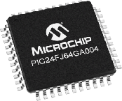
TQFP-44
描述:
MICROCHIP PIC24FJ64GA004-I/PT 微控制器, 16位, 通用, PIC24FJ, 32 MHz, 64 KB, 8 KB, 44 引脚, TQFP
Pictures:
3D模型
符号图
焊盘图
引脚图
产品图
页面导航:
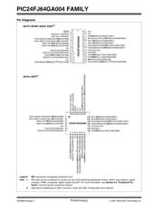
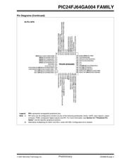
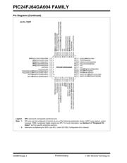
引脚图在P4P5P6P13P14P15P16P17P18P193P206Hot
原理图在P12P20P49P99P119P122P123P127P132P135P136P137
封装尺寸在P241
标记信息在P239
封装信息在P226P239P241P242P243P244P245P246P255
功能描述在P163
技术参数、封装参数在P227P231P232P233P235P237
电气规格在P210
导航目录
PIC24FJ64GA004-I/PT数据手册
Page:
of 256 Go
若手册格式错乱,请下载阅览PDF原文件
© 2007 Microchip Technology Inc. Preliminary DS39881B-page 1
PIC24FJ64GA004 FAMILY
High-Performance CPU:
• Modified Harvard Architecture
• Up to 16 MIPS Operation @ 32 MHz
• 8 MHz Internal Oscillator with 4x PLL Option and
Multiple Divide Options
• 17-Bit by 17-Bit Single-Cycle Hardware Multiplier
• 32-Bit by 16-Bit Hardware Divider
• 16-Bit x 16-Bit Working Register Array
• C Compiler Optimized Instruction Set Architecture:
- 76 base instructions
- Flexible addressing modes
• Two Address Generation Units for Separate Read
and Write Addressing of Data Memory
Special Microcontroller Features:
• Operating Voltage Range of 2.0V to 3.6V
• 5.5V Tolerant Input (digital pins only)
• High-Current Sink/Source (18 mA/18 mA) on All I/O Pins
• Flash Program Memory:
- 10,000 erase/write
- 20-year data retention minimum
• Power Management modes:
- Sleep, Idle, Doze and Alternate Clock modes
- Operating current 650
μ
A/MIPS typical at 2.0V
- Sleep current 150 nA typical at 2.0V
• Fail-Safe Clock Monitor Operation:
- Detects clock failure and switches to on-chip,
low-power RC oscillator
• On-Chip, 2.5V Regulator with Tracking mode
• Power-on Reset (POR), Power-up Timer (PWRT)
and Oscillator Start-up Timer (OST)
• Flexible Watchdog Timer (WDT) with On-Chip,
Low-Power RC Oscillator for Reliable Operation
• In-Circuit Serial Programming™ (ICSP™) and
In-Circuit Debug (ICD) via 2 Pins
• JTAG Boundary Scan and Programming Support
Analog Features:
• 10-Bit, up to 13-Channel Analog-to-Digital Converter:
- 500 ksps conversion rate
- Conversion available during Sleep and Idle
• Dual Analog Comparators with Programmable
Input/Output Configuration
Peripheral Features:
• Peripheral Pin Select:
- Allows independent I/O mapping of many peripherals
- Up to 26 available pins (44-pin devices)
- Continuous hardware integrity checking and safety
interlocks prevent unintentional configuration changes
• 8-Bit Parallel Master/Slave Port (PMP/PSP):
- Up to 16-bit multiplexed addressing, with up to
11 dedicated address pins on 44-pin devices
- Programmable polarity on control lines
• Hardware Real-Time Clock/Calendar (RTCC):
- Provides clock, calendar and alarm functions
• Programmable Cyclic Redundancy Check (CRC)
• Two 3-Wire/4-Wire SPI modules (support 4 Frame
modes) with 8-Level FIFO Buffer
•Two I
2
C™ modules support Multi-Master/Slave
mode and 7-Bit/10-Bit Addressing
• Two UART modules:
- Supports RS-485, RS-232, and LIN 1.2
- On-chip hardware encoder/decoder for IrDA
®
- Auto-wake-up on Start bit
- Auto-Baud Detect
- 4-level deep FIFO buffer
• Five 16-Bit Timers/Counters with Programmable Prescaler
• Five 16-Bit Capture Inputs
• Five 16-Bit Compare/PWM Outputs
• Configurable Open-Drain Outputs on Digital I/O Pins
• Up to 4 External Interrupt Sources
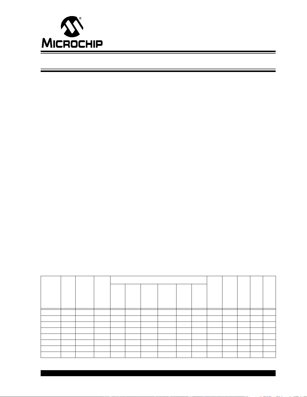
PIC24FJ
Device
Pins
Program
Memory
(bytes)
SRAM
(bytes)
Remappable Peripherals
I
2
C™
10-Bit A/D
(ch)
Comparators
PMP/PSP
JTAG
Remappable
Pins
Timers
16-Bit
Capture
Input
Compare/
PWM
Output
UART w/
IrDA
®
SPI
16GA002 28 16K 4K 16 5 5 5 2 2 2 10 2 Y Y
32GA002 28 32K 8K 16 5 5 5 2 2 2 10 2 Y Y
48GA002 28 48K 8K 16 5 5 5 2 2 2 10 2 Y Y
64GA002 28 64K 8K 16 5 5 5 2 2 2 10 2 Y Y
16GA004 44 16K 4K 26 5 5 5 2 2 2 13 2 Y Y
32GA004 44 32K 8K 26 5 5 5 2 2 2 13 2 Y Y
48GA004 44 48K 8K 26 5 5 5 2 2 2 13 2 Y Y
64GA004 44 64K 8K 26 5 5 5 2 2 2 13 2 Y Y
28/44-Pin General Purpose, 16-Bit Flash Microcontrollers
器件 Datasheet 文档搜索
AiEMA 数据库涵盖高达 72,405,303 个元件的数据手册,每天更新 5,000 多个 PDF 文件
