Datasheet 搜索 > 微控制器 > Renesas Electronics(瑞萨电子) > R5F100FEAFP#V0 数据手册 > R5F100FEAFP#V0 其他数据使用手册 1/202 页
 器件3D模型
¥ 7.394
R5F100FEAFP#V0 其他数据使用手册 - Renesas Electronics(瑞萨电子)
制造商:
Renesas Electronics(瑞萨电子)
分类:
微控制器
封装:
LQFP-44
描述:
RL78/G13, 16-Bit Microcontrollers, 64kB/96kB Flash, Renesas ElectronicsRL78 is Renesas Electronics" next-generation microcontroller family combining advanced features from both the 78K and R8C families to deliver low power consumption (66uA / MHz) and high performance (41DMIPS @ 32MHz). RL78 is based upon a 16bit CISC architecture with analogue rich functionality. The platform line-up will include general purpose, LCD and ASSPs including lighting and automotive microcontrollers. RL78 is designed specifically for ultra-low power applications enabling customers to build compact and energy-efficient systems at lower cost. In addition to a high-precision (±1%) on-chip oscillator enabling 32MHz CPU operation and other standard on-chip functions from the RL78/G13, the RL78/G14 microcontrollers have multiply, divide and multiply-accumulate instructions capable of faster processing than the RL78/G13, and functions from the R8C Family with proven track records, such as timers RD/RG/RJ, data transfer controller, and event link controller, helping to lower the total cost of building a system and contributing to more compact size and lower power consumption.### 注Data Flash Memory is Not Mounted.### RL78 系列微控制器,Renesas Electronics### RL78 Family Microcontrollers, Renesas Electronics展开
Pictures:
3D模型
符号图
焊盘图
引脚图
产品图
页面导航:
引脚图在P16Hot
原理图在P34
封装尺寸在P178P179P180P181P182P183P184P185P186P187P188P189
型号编码规则在P4P5P6P7P8P9P10P11P12P13P14P15
封装信息在P3
技术参数、封装参数在P54P55P56P57P58P59P60P61P62P63P64P65
应用领域在P1P124P125P126P127P128P129P130P131P132P133P134
电气规格在P54P55P56P57P58P59P60P61P62P63P64P65
型号编号列表在P3P4P5P6P7P8P9P10P11P12P13P14
导航目录
R5F100FEAFP#V0数据手册
Page:
of 202 Go
若手册格式错乱,请下载阅览PDF原文件
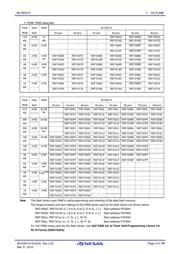
Datasheet
RL78/G13
RENESAS MCU
True Low Power Platform (as low as 66 µA/MHz, and 0.57 µA for RTC + LVD), 1.6 V to 5.5 V
operation, 16 to 512 Kbyte Flash, 41 DMIPS at 32 MHz, for General Purpose Applications
Page 1 of 196
R01DS0131EJ0330
Rev.3.30
Mar 31, 2016
R01DS0131EJ0330 Rev.3.30
Mar 31, 2016
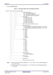
1. OUTLINE
1.1 Features
Ultra-low power consumption technology
V
DD = single power supply voltage of 1.6 to 5.5 V
HALT mode
STOP mode
SNOOZE mode
RL78 CPU core
CISC architecture with 3-stage pipeline
Minimum instruction execution time: Can be changed
from high speed (0.03125 μs: @ 32 MHz operation
with high-speed on-chip oscillator) to ultra-low speed
(30.5 μs: @ 32.768 kHz operation with subsystem
clock)
Address space: 1 MB
General-purpose registers: (8-bit register × 8) × 4
banks
On-chip RAM: 2 to 32 KB
Code flash memory
Code flash memory: 16 to 512 KB
Block size: 1 KB
Prohibition of block erase and rewriting (security
function)
On-chip debug function
Self-programming (with boot swap function/flash
shield window function)
Data Flash Memory
Data flash memory: 4 KB to 8 KB
Back ground operation (BGO): Instructions can be
executed from the program memory while rewriting
the data flash memory.
Number of rewrites: 1,000,000 times (TYP.)
Voltage of rewrites: V
DD = 1.8 to 5.5 V
High-speed on-chip oscillator
Select from 32 MHz, 24 MHz, 16 MHz, 12 MHz, 8
MHz, 6 MHz, 4 MHz, 3 MHz, 2 MHz, and 1 MHz
High accuracy: +/- 1.0 % (V
DD = 1.8 to 5.5 V, TA = -20
to +85°C)
Operating ambient temperature
T
A = -40 to +85°C (A: Consumer applications, D:
Industrial applications )
T
A = -40 to +105°C (G: Industrial applications)
Power management and reset function
On-chip power-on-reset (POR) circuit
On-chip voltage detector (LVD) (Select interrupt and
reset from 14 levels)
DMA (Direct Memory Access) controller
2/4 channels
Number of clocks during transfer between 8/16-bit
SFR and internal RAM: 2 clocks
Multiplier and divider/multiply-accumulator
16 bits × 16 bits = 32 bits (Unsigned or signed)
32 bits ÷ 32 bits = 32 bits (Unsigned)
16 bits × 16 bits + 32 bits = 32 bits (Unsigned or
signed)
Serial interface
CSI: 2 to 8 channels
UART/UART (LIN-bus supported): 2 to 4 channels
I
2
C/Simplified I
2
C communication: 2 to 8 channels
Timer
16-bit timer: 8 to 16 channels
12-bit interval timer: 1 channel
Real-time clock: 1 channel (calendar for 99
years, alarm function, and
clock correction function)
Watchdog timer: 1 channel (operable with the
dedicated low-speed on-chip
oscillator)
A/D converter
8/10-bit resolution A/D converter (V
DD = 1.6 to 5.5 V)
Analog input: 6 to 26 channels
Internal reference voltage (1.45 V) and temperature
sensor
Note 1
I/O port
I/O port: 16 to 120 (N-ch open drain I/O [withstand
voltage of 6 V]: 0 to 4, N-ch open drain I/O
[V
DD withstand voltage
Note 2
/EVDD withstand
voltage
Note 3
]: 5 to 25)
Can be set to N-ch open drain, TTL input buffer, and
on-chip pull-up resistor
Different potential interface: Can connect to a
1.8/2.5/3 V device
On-chip key interrupt function
On-chip clock output/buzzer output controller
Others
On-chip BCD (binary-coded decimal) correction
circuit
Notes 1. Can be selected only in HS (high-speed
main) mode
2. Products with 20 to 52 pins
3. Products with 64 to 128 pins
Remark The functions mounted depend on the
product. See 1.6 Outline of Functions.
器件 Datasheet 文档搜索
AiEMA 数据库涵盖高达 72,405,303 个元件的数据手册,每天更新 5,000 多个 PDF 文件
