Datasheet 搜索 > TVS二极管 > Vishay Semiconductor(威世) > RS1D-13 数据手册 > RS1D-13 其他数据使用手册 1/3 页

¥ 0
RS1D-13 其他数据使用手册 - Vishay Semiconductor(威世)
制造商:
Vishay Semiconductor(威世)
分类:
TVS二极管
封装:
DO-214AC
Pictures:
3D模型
符号图
焊盘图
引脚图
产品图
RS1D-13数据手册
Page:
of 3 Go
若手册格式错乱,请下载阅览PDF原文件
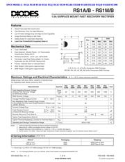
DS15002 Rev. 10 - 2 1 of 3 RS1A/B - RS1M/B
www.diodes.com
ã Diodes Incorporated
RS1A/B - RS1M/B
1.0A SURFACE MOUNT FAST RECOVERY RECTIFIER
Features
A, B, D, G, J, K, M Suffix Designates SMA Package
AB, BB, DB, GB, JB, KB, MB Suffix Designates SMB Package
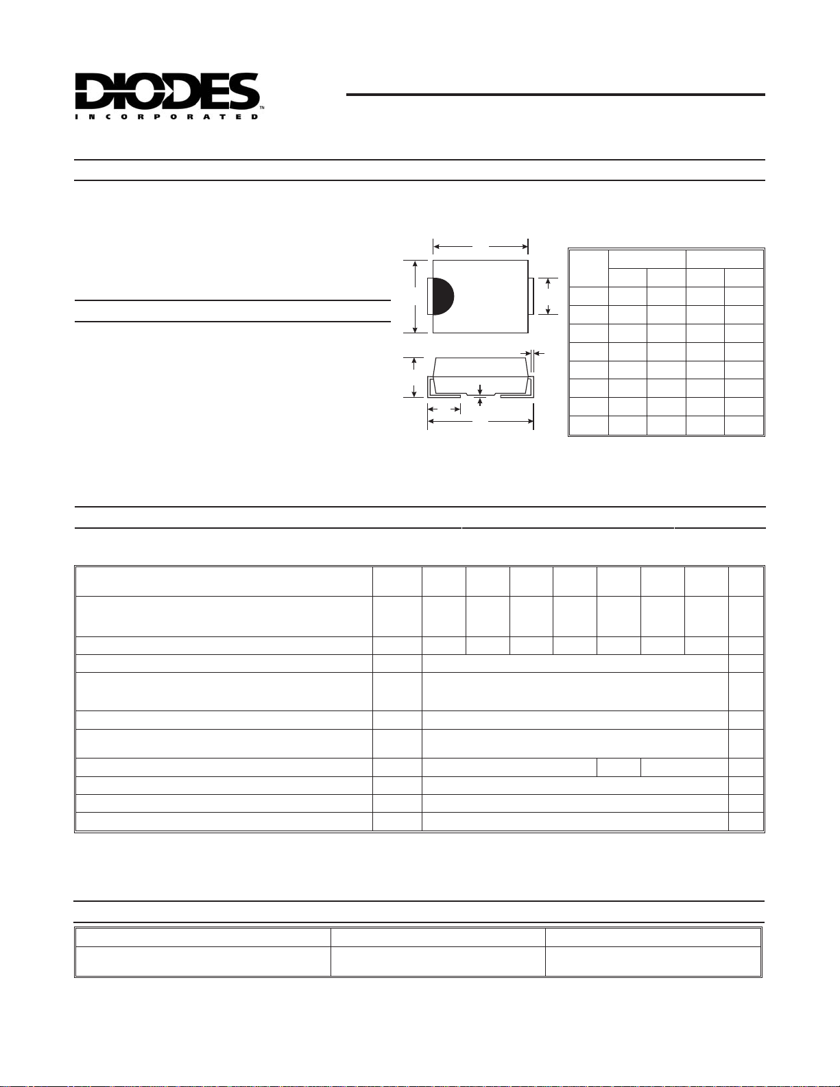
Dim
SMA SMB
Min Max Min Max
A
2.29 2.92 3.30 3.94
B
4.00 4.60 4.06 4.57
C
1.27 1.63 1.96 2.21
D
0.15 0.31 0.15 0.31
E
4.80 5.59 5.00 5.59
G
0.10 0.20 0.10 0.20
H
0.76 1.52 0.76 1.52
J
2.01 2.30 2.00 2.40
A
B
C
D
G
H
E
J
·
Glass Passivated Die Construction
·
Fast Recovery Time For High Efficiency
·
Low Forward Voltage Drop and High Current Capability
·
Surge Overload Rating to 30A Peak
·
Ideally Suited for Automated Assembly
·
Lead Free Finish/RoHS Compliant (Note 4)
Mechanical Data
·
Case: SMA/SMB
·
Case Material: Molded Plastic. UL Flammability
Classification Rating 94V-0
·
Moisture Sensitivity: Level 1 per J-STD-020C
·
Terminals: Lead Free Plating (Matte Tin Finish).
Solderable per MIL-STD-202, Method 208
·
Polarity: Cathode Band or Cathode Notch
·
SMA Weight: 0.064 grams (approximate)
·
SMB Weight: 0.093 grams (approximate)
Maximum Ratings and Electrical Characteristics
@ T
A
= 25°C unless otherwise specified
Single phase, half wave, 60Hz, resistive or inductive load.
For capacitive load, derate current by 20%.
Notes: 1. Valid provided that terminals are kept at ambient temperature.
2. Measured at 1.0MHz and applied reverse voltage of 4.0V DC.
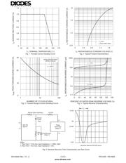
3. Reverse Recovery Test Conditions: I
F
= 0.5A, I
R
= 1.0A, I
rr
= 0.25A. See figure 5.
4. RoHS revision 13.2.2003. Glass and High Temperature Solder Exemptions Applied, see
EU Directive Annex Notes 5 and 7.
Characteristic Symbol
RS1
A/AB
RS1
B/BB
RS1
D/DB
RS1
G/GB
RS1
J/JB
RS1
K/KB
RS1
M/MB
Unit
Peak Repetitive Reverse Voltage
Working Peak Reverse Voltage
DC Blocking Voltage
V
RRM
V
RWM
V
R
50 100 200 400 600 800 1000 V
RMS Reverse Voltage
V
R(RMS)
35 70 140 280 420 560 700 V
Average Rectified Output Current @ T
T
= 120°C
I
O
1.0 A
Non-Repetitive Peak Forward Surge Current,
8.3ms single half sine-wave Superimposed on Rated Load
(JEDEC Method)
I
FSM
30 A
Forward Voltage Drop @ I
F
= 1.0A
V
FM
1.3 V
Peak Reverse Current @ T
A
= 25°C
at Rated DC Blocking Voltage @ T
A
= 125°C
I
RM
5.0
200
µA
Reverse Recovery Time (Note 3)
t
rr
150 250 500 ns
Typical Total Capacitance (Note 2)
C
T
15 pF
Typical Thermal Resistance, Junction to Terminal (Note 1)
R
qJT
20 °C/W
Operating and Storage Temperature Range
T
j,
T
STG
-65 to +150 °C
Device*
Packaging Shipping
RS1x-13-F
RS1xB-13-F
SMA
SMB
5000/Tape & Reel
3000/Tape & Reel
Ordering Information
* x = Device type, e.g. RS1D-13-F (SMA package); RS1JB-13-F (SMB package).
Notes: 5. For Packaging Details, go to our website at http://www.diodes.com/datasheets/ap02007.pdf.
(Note 5 & 6)
SPICE MODELS: RS1A RS1B RS1D RS1G RS1J RS1K RS1M RS1AB RS1BB RS1DB RS1GB RS1JB RS1KB RS1MB
器件 Datasheet 文档搜索
AiEMA 数据库涵盖高达 72,405,303 个元件的数据手册,每天更新 5,000 多个 PDF 文件
