Datasheet 搜索 > 二极管阵列 > Microsemi(美高森美) > SMDA03C/TR7 数据手册 > SMDA03C/TR7 其他数据使用手册 1/2 页

 器件3D模型
¥ 8.659
SMDA03C/TR7 其他数据使用手册 - Microsemi(美高森美)
制造商:
Microsemi(美高森美)
分类:
二极管阵列
封装:
SO-8
Pictures:
3D模型
符号图
焊盘图
引脚图
产品图
页面导航:
应用领域在P1
导航目录
SMDA03C/TR7数据手册
Page:
of 2 Go
若手册格式错乱,请下载阅览PDF原文件

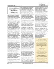
Spring/Summer 1998
20
Fax On Demand (800)713-4113
Component SPICE modeling has
become a frequently used analysis
tool by design engineers to evaluate
circuit performance. This MicroNote
provides background information and
methods useful for quickly obtaining
many of the discrete diode SPICE
parameters such as BV, IBV, IS, EG,
TBV1, etc. from either specified data
sheet parameters or other known
information. Others may be
approximated as described herein or
obtained from the manufacturing
source with other related physical
design or characteristic background
information. The SPICE parameters
for diodes described in this
MicroNote begin with the reverse
diode characteristics and conclude
with the forward parameter features.
For quick reference, each of the
SPICE parameter acronyms are
underlined and are then described in
further detail.
In our first example of BV for reverse
breakdown knee voltage, this simply
approximates the avalanche
breakdown voltage or what has been
identified in data sheets as “V
BR
” for
Rectifiers and Transient Voltage
Suppressors (TVSs) or “V
Z
” for zener
diodes. If the V
BR
parameter is not
specified for rectifiers, it may be
approximated as somewhat higher
than the commonly rated reverse
voltage (V
RWM
) of a rectifier. A 10 to
20% higher value is typical for “fast”
and “ultrafast” Rectifiers or Schottkys.
For lower voltage “standard” rectifiers
in a JEDEC registered series where
reverse recovery time is not critical
(e.g. 1N4000 series), the actual V
BR
can be many times higher than rated
V
RWM
. This occurs when rectifiers are
downgraded from higher voltages in
a series by a manufacturer where all
other parameters (such as forward
voltage) are identical in ratings.
The IBV that represents reverse
breakdown knee current for onset of
breakdown voltage can be
approximated as ten times greater
than the maximum specified leakage
current (I
R
). In other examples for a
conservative or worst case (highest)
value, this may instead be specified
as I
ZK
for knee current on zeners or I
BR
(sometimes listed as I
T
) for TVSs. It
may also simply be those values
shown separately for the V
BR
current
on some signal/switching diode data
sheets. Many of these latter
examples often specify the V
BR
at
100 µA that is applicable for IBV.
The saturation current IS may be
approximated as the “process norm”
of the leakage current in large-scale
signal dc modeling with SPICE. This
may be further represented in data
sheets by I
R
for rectifiers or zeners
and I
D
for TVSs. For glass passivated
pn junction designs (as primarily
offered by Microsemi), this may
typically be 10% to 20% of maximum
leakage current specified for diodes
in many of the 1NXXXX JEDEC
registrations. For a worst case
(highest value) scenario, it can also
be simply modeled as the maximum
leakage current I
R
(or I
D
) value
specified. This may be in the range
of 10
-8
to 10
-5
Amps depending on
size of the diode. For low voltage
zeners or TVSs that do not avalanche
with a sharp knee region, the leakage
current or saturation current
approaches that of the rated
maximum I
R
of zeners or I
D
of a TVS.
This can sometimes approach 100 to
5000 µA (10
-4
to 5x10
-3
A) again
depending on size of the device.
If the IS value is needed for a linearized
small-signal ac SPICE model, then this
would equate to smaller saturation
current values when measured at
0.026 volts (kT/q). This results in very
low IS values in the 10
-9
to 10
-15
Amps
range (or nA to fA) depending on size of
the diode.
The zero bias pn junction capacitance
CJO is also often specified in various
diode data sheets. This may simply be
shown as “C” if also stated at zero
volts. If not, it will require direct
measurement or further information
from the manufacturing source.
Much like a parallel plate capacitor,
the diode capacitance will be dictated
by its pn junction area size and
depletion layer spread (or plate
separation). This results in higher
capacitance for larger size rectifiers
(or Schottkys) as well as zeners and
TVSs. It is similarly dependent on the
actual voltage V
Z
or V
BR
(or effective
plate separation). The higher the
actual voltage...the lower the
capacitance. This is particularly
evident when comparing the
capacitance for an overall family
series listing of zeners or TVSs
where low voltage devices are
depicted with much higher
capacitance than high voltage types.
The pn grading coefficient M further
characterizes sensitivity of
capacitance and its decline with
applied reverse voltage on a
logarithmic scale. It is not directly
shown on data sheets, but the
effective M values generally lie
between the value of 0.25 to 0.45 for
most conventional pn junction
diodes. Low voltage zeners below 5
volts using alloy-diffused pn junction
technology may only have an M value of
0.25 whereas higher voltage zeners (50
to 100 volts) may be 0.35. Higher
voltage rectifiers of many hundreds of
volts may approach 0.45. An abrupt
junction or Schottky diode has an M
How to Quickly Obtain Spice
Parameters for Diodes
MicroNote
Series 010
by Kent Walters, Microsemi Corporate Applications
器件 Datasheet 文档搜索
AiEMA 数据库涵盖高达 72,405,303 个元件的数据手册,每天更新 5,000 多个 PDF 文件


