Datasheet 搜索 > 开发套件 > TI(德州仪器) > SN65CML100EVM 数据手册 > SN65CML100EVM 其他数据使用手册 1/19 页

¥ 852.96
SN65CML100EVM 其他数据使用手册 - TI(德州仪器)
制造商:
TI(德州仪器)
分类:
开发套件
描述:
TEXAS INSTRUMENTS SN65CML100EVM 评估板, SN65CML100 转换器/中继器
Pictures:
3D模型
符号图
焊盘图
引脚图
产品图
页面导航:
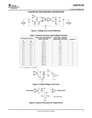
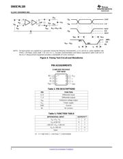
引脚图在P6Hot
典型应用电路图在P1P11
原理图在P7
封装尺寸在P12P14P15
型号编码规则在P2
标记信息在P2P12P13
封装信息在P12P13P14P15
技术参数、封装参数在P2
应用领域在P1P19
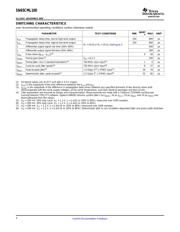
电气规格在P3
导航目录
SN65CML100EVM数据手册
Page:
of 19 Go
若手册格式错乱,请下载阅览PDF原文件
www.ti.com
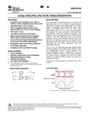
FEATURES DESCRIPTION
APPLICATIONS
FUNCTIONAL DIAGRAM
8
2
3
4
7
6
V
CC
A
B
V
BB
Y
Z
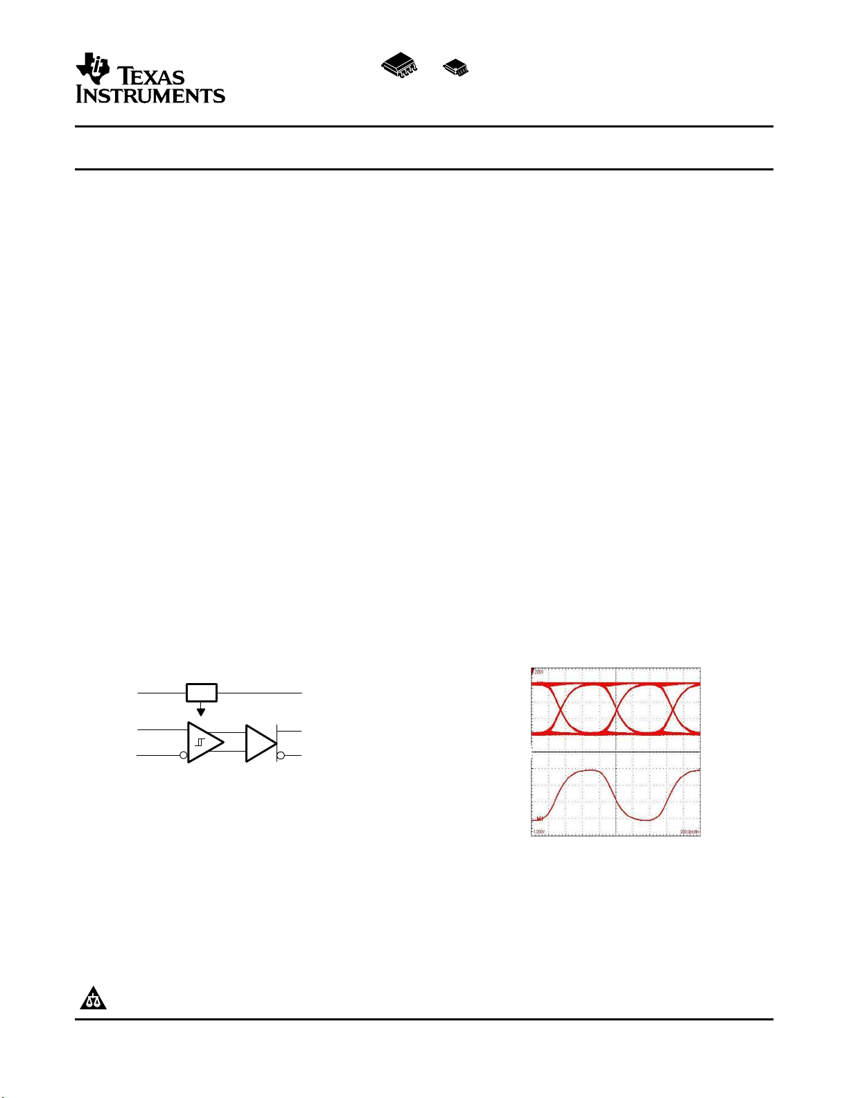
EYE PATTERN
1.5 Gbps
2
23
-1 PRBS
750 MHz
V
CC
= 3.3 V, T
A
= 25°C, V
ID
= 200 mV, V
IC
= 1.2 V, V
TT
= 3.3 V, R
T
= 50 Ω
Vertical Scale = 500 mV/div
Horizontal Scale = 200 ps/div
SN65CML100
SLLS547 – NOVEMBER 2002
1.5-Gbps LVDS/LVPECL/CML-TO-CML TRANSLATOR/REPEATER
• Provides Level Translation From LVDS or
This high-speed translator/repeater is designed for
LVPECL to CML, Repeating From CML to CML
signaling rates up to 1.5 Gbps to support various
high-speed network routing applications. The driver
• Signaling Rates
(1)
up to 1.5 Gbps
output is compatible with current-mode logic (CML)
• CML Compatible Output Directly Drives
levels, and directly drives 50- Ω or 25- Ω loads
Devices With 3.3-V, 2.5-V, or 1.8-V Supplies
connected to 1.8-V, 2.5-V, or 3.3-V nominal supplies.
• Total Jitter < 70 ps
The capability for direct connection to the loads may
eliminate the need for coupling capacitors. The
• Low 100 ps (Max) Part-To-Part Skew
receiver input is compatible with LVDS (TIA/EIA-644),
• Wide Common-Mode Receiver Capability
LVPECL, and CML signaling levels. The receiver
Allows Direct Coupling of Input Signals
tolerates a wide common-mode voltage range, and
• 25 mV of Receiver Input Threshold Hysteresis
may also be directly coupled to the signal source.
Over 0-V to 4-V Common-Mode Range
The internal data path from input to output is fully
differential for low noise generation and low
• Propagation Delay Times, 800 ps Maximum
pulse-width distortion.
• 3.3-V Supply Operation
The V
BB
pin is an internally generated voltage supply
• Available in SOIC and MSOP Packages
to allow operation with a single-ended LVPECL input.
For single-ended LVPECL input operation, the
unused differential input is connected to V
BB
as a
• Level Translation
switching reference voltage. When used, decouple
• 622-MHz Central Office Clock Distribution
V
BB
with a 0.01- µ F capacitor and limit the current
sourcing or sinking to 400 µ A. When not used, V
BB• High-Speed Network Routing
should be left open.
• Wireless Basestations
This device is characterized for operation from –40 ° C
• Low Jitter Clock Repeater
(1)
to 85 ° C.
(1) The signaling rate of a line is the number of voltage
transitions that are made per second expressed in the units
bps (bits per second).
Please be aware that an important notice concerning availability, standard warranty, and use in critical applications of Texas
Instruments semiconductor products and disclaimers thereto appears at the end of this data sheet.
PRODUCTION DATA information is current as of publication date.
Copyright © 2002–TBD, Texas Instruments Incorporated
Products conform to specifications per the terms of the Texas
Instruments standard warranty. Production processing does not
necessarily include testing of all parameters.
器件 Datasheet 文档搜索
AiEMA 数据库涵盖高达 72,405,303 个元件的数据手册,每天更新 5,000 多个 PDF 文件
