Datasheet 搜索 > 触发器 > TI(德州仪器) > SN74AC74MDREP 数据手册 > SN74AC74MDREP 其他数据使用手册 1/9 页
 器件3D模型
¥ 16.183
SN74AC74MDREP 其他数据使用手册 - TI(德州仪器)
制造商:
TI(德州仪器)
分类:
触发器
封装:
SOIC-14
描述:
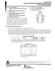
双上升沿触发的D型触发器具有清零和预设 DUAL POSITIVE-EDGE-TRIGGERED D-TYPE FLIP-FLOP WITH CLEAR AND PRESET
Pictures:
3D模型
符号图
焊盘图
引脚图
产品图
页面导航:
导航目录
SN74AC74MDREP数据手册
Page:
of 9 Go
若手册格式错乱,请下载阅览PDF原文件
SCAS721 − OCTOBER 2003
1
POST OFFICE BOX 655303 • DALLAS, TEXAS 75265
D Controlled Baseline
− One Assembly/Test Site, One Fabrication
Site
D Extended Temperature Performance of
−55°C to 125°C
D Enhanced Diminishing Manufacturing
Sources (DMS) Support
D Enhanced Product-Change Notification
D Qualification Pedigree
†
†
Component qualification in accordance with JEDEC and industry
standards to ensure reliable operation over an extended
temperature range. This includes, but is not limited to, Highly
Accelerated Stress Test (HAST) or biased 85/85, temperature
cycle, autoclave or unbiased HAST, electromigration, bond
intermetallic life, and mold compound life. Such qualification
testing should not be viewed as justifying use of this component
beyond specified performance and environmental limits.
D 2-V to 6-V V
CC
Operation
D Inputs Accept Voltages to 6 V
D Max t
pd
of 10 ns at 5 V
description/ordering information
The SN74AC74 is a dual positive-edge-triggered D-type flip-flop.
A low level at the preset (PRE
) or clear (CLR) input sets or resets the outputs, regardless of the levels of the
other inputs. When PRE
and CLR are inactive (high), data at the data (D) input meeting the setup-time
requirements is transferred to the outputs on the positive-going edge of the clock pulse. Clock triggering occurs
at a voltage level and is not directly related to the rise time of the clock pulse. Following the hold-time interval,
data at D can be changed without affecting the levels at the outputs.
ORDERING INFORMATION
T
A
PACKAGE
‡
ORDERABLE
PART NUMBER
TOP-SIDE
MARKING
−55°C to 125°C SOIC − D Tape and reel SN74AC74MDREP SAC74MEP
‡
Package drawings, standard packing quantities, thermal data, symbolization, and PCB design guidelines are
available at www.ti.com/sc/package.
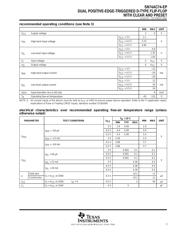
FUNCTION TABLE
INPUTS
OUTPUTS
PRE
CLR
CLK D Q Q
L H X X H L
H LXXLH
L LXXH
§
H
§
H H ↑ HHL
H H ↑ LLH
H H L X Q
0
Q
0
§
This configuration is nonstable; that is, it does not
persist when either PRE
or CLR returns to its
inactive (high) level.
Copyright 2003, Texas Instruments Incorporated
!"# $"%&! '#(
'"! ! $#!! $# )# # #* "#
'' +,( '"! $!#- '# #!#&, !&"'#
#- && $##(
Please be aware that an important notice concerning availability, standard warranty, and use in critical applications o
f
Texas Instruments semiconductor products and disclaimers thereto appears at the end of this data sheet.
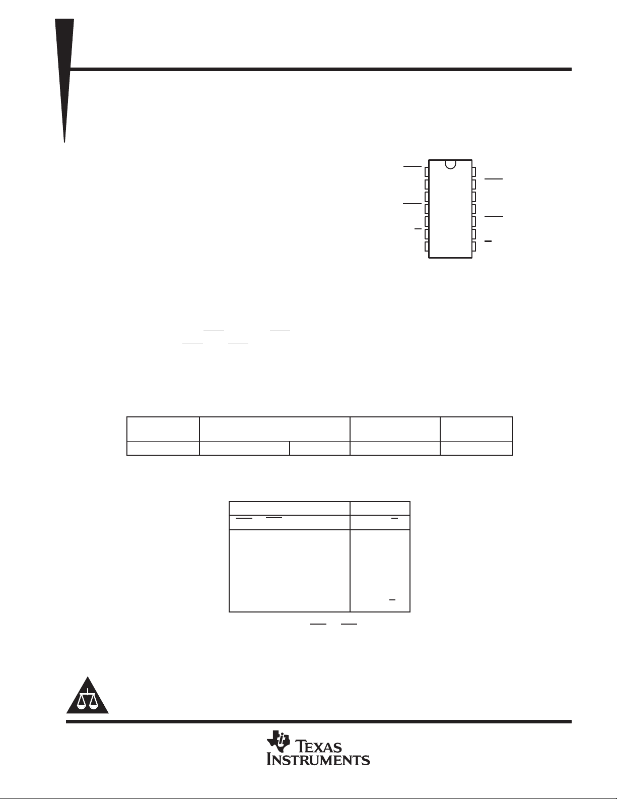
1
2
3
4
5
6
7
14
13
12
11
10
9
8
1CLR
1D
1CLK
1PRE
1Q
1Q
GND
V
CC
2CLR
2D
2CLK
2PRE
2Q
2Q
D PACKAGE
(TOP VIEW)
器件 Datasheet 文档搜索
AiEMA 数据库涵盖高达 72,405,303 个元件的数据手册,每天更新 5,000 多个 PDF 文件
