Datasheet 搜索 > 微控制器 > ST Microelectronics(意法半导体) > STM32F102C6T6A 数据手册 > STM32F102C6T6A 其他数据使用手册 6/79 页
 器件3D模型
¥ 1.168
STM32F102C6T6A 其他数据使用手册 - ST Microelectronics(意法半导体)
制造商:
ST Microelectronics(意法半导体)
分类:
微控制器
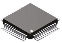
封装:
LQFP-48
描述:
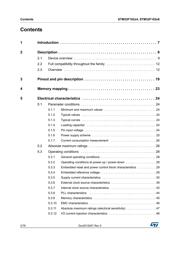
STM32F102 系列微处理器,STMicroelectronicsST 的 STM32F102 MCU 系列 ARM Cortex™ M3、32 位 RISC 内核运行频率高达 48MHz,带高达 128 KB 的高速闪存、高达 16 KB 的 SRAM 以及增强型外设。 ARM™ 处理器 STM32 F102 32 位微控制器具有一个通信接口;计时器;ADC 和 DAC。 STM32 系列 ARM Cortex-M3 32 位闪存产品系列以低功率、低电压运行,并结合了带实时功能的高性能,可以在 STMicroelectronics STM32 平台上运行。 微控制器可用于如应用控制、消费者电器用具、PC 外设、手持设备、HVAC 及其他许多应用领域。 48 MHz CPU,带 USB FS 电源:2 V 至 3.6 V 通信接口:I2C、SPI、USART 12 位 ADC;16 位计时器 温度范围:-40 至 +85 °C ### STM32F1 系列 32 位 ARM® Cortex®-M3 微控制器,STMicroelectronics32 位闪存微控制器的 STM32 系列基于 ARM Cortex™ M3 核心的突破 - 为嵌入式应用特别开发的核心。 STM32 系列得益于 Cortex-M3 体系结构增强功能,包括为传达改进性能而设置的 Thumb-2 指令,带更好的编码密度,对中断更快的反应,所有的均和领先的工业功耗相接合。出色的实时表现 卓越功效 卓越的和新型的外围设备 最大程度的集成 跨族引脚,外围设备和软件兼容性展开
Pictures:
3D模型
符号图
焊盘图
引脚图
产品图
页面导航:
典型应用电路图在P42P43P65
封装尺寸在P68P72
型号编码规则在P74P75
封装信息在P67P68P69P70P71P72P73P74
功能描述在P1P8P9P10P11P12P13P14P15P16P17P18
技术参数、封装参数在P26P47
电气规格在P24P25P26P27P28P29P30P31P32P33P34P35
导航目录
STM32F102C6T6A数据手册
Page:
of 79 Go
若手册格式错乱,请下载阅览PDF原文件

List of figures STM32F102x4, STM32F102x6
6/78 DocID15057 Rev 5
List of figures
Figure 1. STM32F102T8 medium-density USB access line block diagram . . . . . . . . . . . . . . . . . . . . 10
Figure 2. Clock tree . . . . . . . . . . . . . . . . . . . . . . . . . . . . . . . . . . . . . . . . . . . . . . . . . . . . . . . . . . . . . . 11
Figure 3. STM32F102xx medium-density USB access line LQFP48 pinout . . . . . . . . . . . . . . . . . . . 19
Figure 4. STM32F102xx medium-density USB access line LQFP64 pinout . . . . . . . . . . . . . . . . . . . 19
Figure 5. Memory map . . . . . . . . . . . . . . . . . . . . . . . . . . . . . . . . . . . . . . . . . . . . . . . . . . . . . . . . . . . . 23
Figure 6. Pin loading conditions . . . . . . . . . . . . . . . . . . . . . . . . . . . . . . . . . . . . . . . . . . . . . . . . . . . . . 25
Figure 7. Pin input voltage . . . . . . . . . . . . . . . . . . . . . . . . . . . . . . . . . . . . . . . . . . . . . . . . . . . . . . . . . 25
Figure 8. Power supply scheme. . . . . . . . . . . . . . . . . . . . . . . . . . . . . . . . . . . . . . . . . . . . . . . . . . . . . 25
Figure 9. Current consumption measurement scheme . . . . . . . . . . . . . . . . . . . . . . . . . . . . . . . . . . . 26
Figure 10. Typical current consumption in Run mode versus temperature (at 3.6 V) -
code with data processing running from RAM, peripherals enabled. . . . . . . . . . . . . . . . . . 32
Figure 11. Typical current consumption in Run mode versus temperature (at 3.6 V) -
code with data processing running from RAM, peripherals disabled . . . . . . . . . . . . . . . . . 32
Figure 12. Typical current consumption on V
BAT
with RTC on versus temperature at different
V
BAT
values . . . . . . . . . . . . . . . . . . . . . . . . . . . . . . . . . . . . . . . . . . . . . . . . . . . . . . . . . . . . 34
Figure 13. Typical current consumption in Stop mode with regulator in Run mode versus
temperature at V
DD
= 3.3 V and 3.6 V . . . . . . . . . . . . . . . . . . . . . . . . . . . . . . . . . . . . . . . . 34
Figure 14. Typical current consumption in Stop mode with regulator in Low-power mode versus
temperature at V
DD
= 3.3 V and 3.6 V . . . . . . . . . . . . . . . . . . . . . . . . . . . . . . . . . . . . . . . . 35
Figure 15. Typical current consumption in Standby mode versus temperature at V
DD
= 3.3 V and
3.6 V . . . . . . . . . . . . . . . . . . . . . . . . . . . . . . . . . . . . . . . . . . . . . . . . . . . . . . . . . . . . . . . . . . 35
Figure 16. High-speed external clock source AC timing diagram . . . . . . . . . . . . . . . . . . . . . . . . . . . . 40
Figure 17. Low-speed external clock source AC timing diagram. . . . . . . . . . . . . . . . . . . . . . . . . . . . . 40
Figure 18. Typical application with an 8 MHz crystal . . . . . . . . . . . . . . . . . . . . . . . . . . . . . . . . . . . . . . 42
Figure 19. Typical application with a 32.768 kHz crystal . . . . . . . . . . . . . . . . . . . . . . . . . . . . . . . . . . . 43
Figure 20. Standard I/O input characteristics - CMOS port . . . . . . . . . . . . . . . . . . . . . . . . . . . . . . . . . 50
Figure 21. Standard I/O input characteristics - TTL port . . . . . . . . . . . . . . . . . . . . . . . . . . . . . . . . . . . 50
Figure 22. 5 V tolerant I/O input characteristics - CMOS port . . . . . . . . . . . . . . . . . . . . . . . . . . . . . . . 51
Figure 23. 5 V tolerant I/O input characteristics - TTL port . . . . . . . . . . . . . . . . . . . . . . . . . . . . . . . . . 51
Figure 24. I/O AC characteristics definition . . . . . . . . . . . . . . . . . . . . . . . . . . . . . . . . . . . . . . . . . . . . . 54
Figure 25. Recommended NRST pin protection . . . . . . . . . . . . . . . . . . . . . . . . . . . . . . . . . . . . . . . . . 55
Figure 26. I
2
C bus AC waveforms and measurement circuit
(1)
. . . . . . . . . . . . . . . . . . . . . . . . . . . . . . 58
Figure 27. SPI timing diagram - slave mode and CPHA=0 . . . . . . . . . . . . . . . . . . . . . . . . . . . . . . . . . 60
Figure 28. SPI timing diagram - slave mode and CPHA=1
(1)
. . . . . . . . . . . . . . . . . . . . . . . . . . . . . . . 60
Figure 29. SPI timing diagram - master mode
(1)
. . . . . . . . . . . . . . . . . . . . . . . . . . . . . . . . . . . . . . . . . 61
Figure 30. USB timings: definition of data signal rise and fall time . . . . . . . . . . . . . . . . . . . . . . . . . . . 62
Figure 31. ADC accuracy characteristics . . . . . . . . . . . . . . . . . . . . . . . . . . . . . . . . . . . . . . . . . . . . . . . 65
Figure 32. Typical connection diagram using the ADC . . . . . . . . . . . . . . . . . . . . . . . . . . . . . . . . . . . . 65
Figure 33. Power supply and reference decoupling. . . . . . . . . . . . . . . . . . . . . . . . . . . . . . . . . . . . . . . 66
Figure 34. LQFP64 - 64-pin, 10 x 10 mm low-profile quad flat package outline . . . . . . . . . . . . . . . . . 67
Figure 35. LQFP64 - 64-pin, 10 x 10 mm low-profile quad flat package
recommended footprint . . . . . . . . . . . . . . . . . . . . . . . . . . . . . . . . . . . . . . . . . . . . . . . . . . . . 68
Figure 36. LQFP64 marking example (package top view). . . . . . . . . . . . . . . . . . . . . . . . . . . . . . . . . . 69
Figure 37. LQFP48 - 48-pin, 7 x 7 mm low-profile quad flat package outline . . . . . . . . . . . . . . . . . . . 70
Figure 38. LQFP48 - 48-pin, 7 x 7 mm low-profile quad flat package
recommended footprint . . . . . . . . . . . . . . . . . . . . . . . . . . . . . . . . . . . . . . . . . . . . . . . . . . . . 72
Figure 39. LQFP48 marking example (package top view). . . . . . . . . . . . . . . . . . . . . . . . . . . . . . . . . . 72
Figure 40. LQFP64 P
D
max vs. T
A
. . . . . . . . . . . . . . . . . . . . . . . . . . . . . . . . . . . . . . . . . . . . . . . . . . . 74
器件 Datasheet 文档搜索
AiEMA 数据库涵盖高达 72,405,303 个元件的数据手册,每天更新 5,000 多个 PDF 文件
