Datasheet 搜索 > ST Microelectronics(意法半导体) > STM32H743I-EVAL 数据手册 > STM32H743I-EVAL 其他数据使用手册 1/226 页

¥ 3308.452
STM32H743I-EVAL 其他数据使用手册 - ST Microelectronics(意法半导体)
制造商:
ST Microelectronics(意法半导体)
描述:
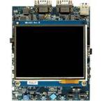
评估板, STM32H743XI MCU, 5.7英寸640x480 TFT彩色LCD, 嵌入式ST-LINK调试器/编程器
Pictures:
3D模型
符号图
焊盘图
引脚图
产品图
页面导航:
引脚图在P47P48P49P50P51P52P53P54P55P56P57P58Hot
典型应用电路图在P119P120P161
封装尺寸在P197P198P199P200P201P202P203P204P205P206P207P208
型号编码规则在P224
技术参数、封装参数在P96P126
电气规格在P94P95P96P97P98P99P100P101P102P103P104P105
导航目录
STM32H743I-EVAL数据手册
Page:
of 226 Go
若手册格式错乱,请下载阅览PDF原文件
This is information on a product in full production.
October 2017 DocID030538 Rev 3 1/226
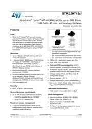
STM32H743xI
32-bit Arm
®
Cortex
®
-M7 400MHz MCUs, up to 2MB Flash,
1MB RAM, 46 com. and analog interfaces
Datasheet - production data
Features
Core
• 32-bit Arm
®
Cortex
®
-M7 core with double-
precision FPU and L1 cache: 16 Kbytes of data
and 16 Kbytes of instruction cache allowing
one cache line to be filled in a single access
from the 256-bit embedded Flash memory;
frequency up to 400 MHz, MPU, 856 DMIPS/
2.14 DMIPS/MHz (Dhrystone 2.1), and DSP
instructions
Memories
• Up to 2 Mbytes of Flash memory with read-
while-write support
• 1 Mbyte of RAM: 192 Kbytes of TCM RAM (inc.
64 Kbytes of ITCM RAM + 128 Kbytes of
DTCM RAM for time critical routines),
864 Kbytes of user SRAM, and 4 Kbytes of
SRAM in Backup domain
• Dual mode Quad-SPI memory interface
running up to 133 MHz
• Flexible external memory controller with up to
32-bit data bus: SRAM, PSRAM,
SDRAM/LPSDR SDRAM, NOR/NAND Flash
clocked up to 133 MHz in synchronous mode
• CRC calculation unit
Security
• ROP, PC-ROP, active tamper
General-purpose input/outputs
• Up to 168 I/O ports with interrupt capability
– Fast I/Os capable of up to 133 MHz
– Up to 164 5 V-tolerant I/Os
Reset and power management
• 3 separate power domains which can be
independently clock gated or switched off to
maximize power efficiency:
– D1: high-performance capabilities for high
bandwidth peripherals
– D2: communication peripherals and timers
– D3: reset/clock control/power management
• 1.62 to 3.6 V application supply and I/Os
• POR, PDR, PVD and BOR
• Dedicated USB power embedding a 3.3 V
internal regulator to supply the internal PHYs
• Embedded regulator (LDO) with configurable
scalable output to supply the digital circuitry
• Voltage scaling in Run and Stop mode (5
configurable ranges)
• Backup regulator (~0.9 V)
• Voltage reference for analog peripheral/V
REF+
• Low-power modes: Sleep, Stop, Standby and
V
BAT
supporting battery charging
Low-power consumption
• Total current consumption down to 4
µA
Clock management
• Internal oscillators: 64 MHz HSI, 48 MHz
HSI48, 4 MHz CSI, 40 kHz LSI
• External oscillators: 4-48 MHz HSE,
32.768 kHz LSE
• 3× PLLs (1 for the system clock, 2 for kernel
clocks) with fractional mode
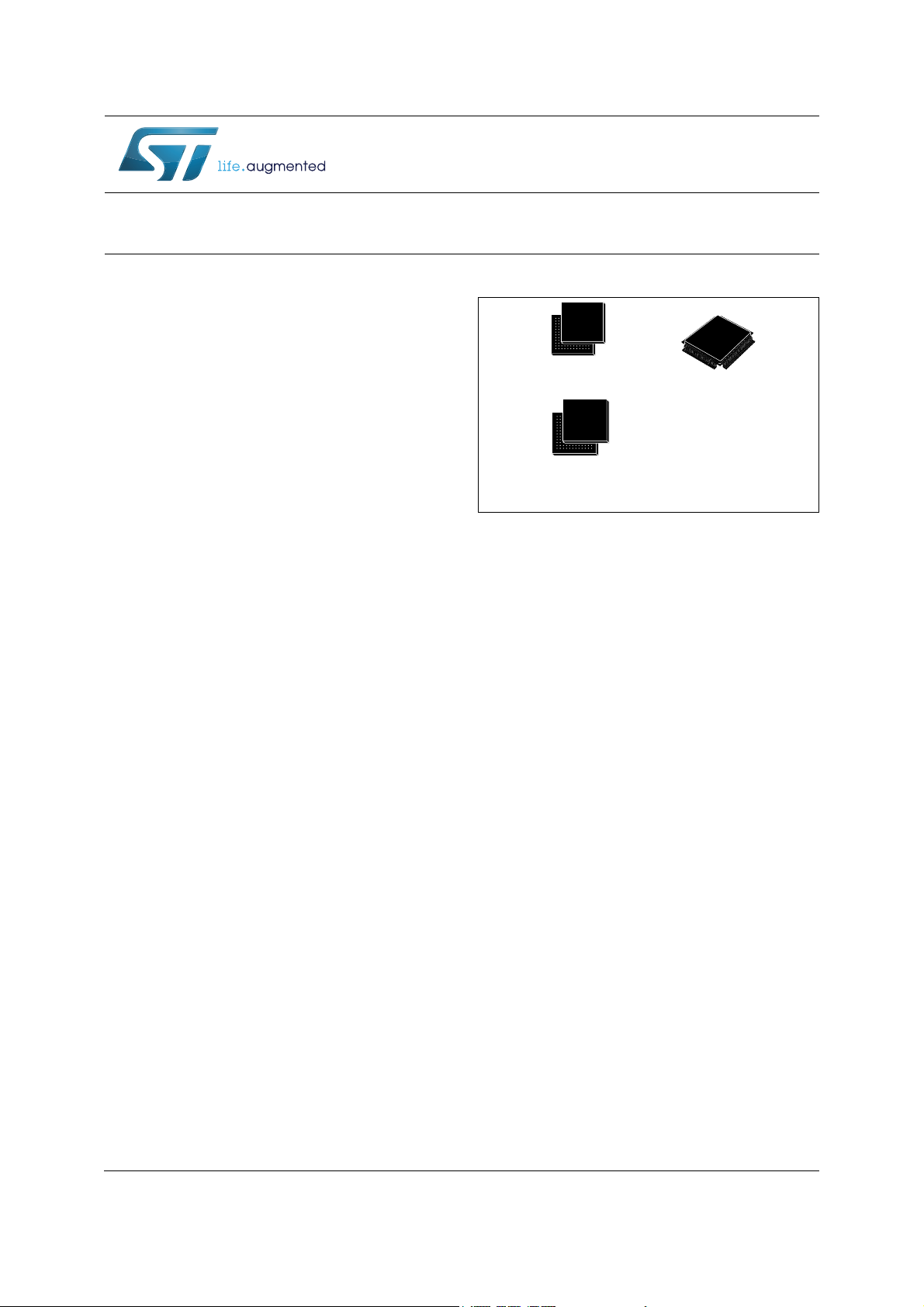
FBGA
LQFP208
(28x28 mm)
LQFP176
(24x24 mm)
LQFP144
(20x20 mm)
LQFP100
(14x14 mm)
UFBGA176+25 (10x10 mm)
UFBGA169 (7x7 mm)
(1)
FBGA
TFBGA240+25 (14x14 mm)
TFBGA100 (8x8 mm)
(1)
1. Package under development.
www.st.com
器件 Datasheet 文档搜索
AiEMA 数据库涵盖高达 72,405,303 个元件的数据手册,每天更新 5,000 多个 PDF 文件
