Datasheet 搜索 > 微控制器 > ST Microelectronics(意法半导体) > STM8S105C6T6 数据手册 > STM8S105C6T6 产品手册 4/127 页


¥ 4.266
STM8S105C6T6 产品手册 - ST Microelectronics(意法半导体)
制造商:
ST Microelectronics(意法半导体)
分类:
微控制器
封装:
LQFP-48
描述:
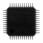
STMICROELECTRONICS STM8S105C6T6 微控制器, 8位, 线路接入, STM8S105xx, 16 MHz, 32 KB, 2 KB, 48 引脚, LQFP
Pictures:
3D模型
符号图
焊盘图
引脚图
产品图
页面导航:
引脚图在P25Hot
典型应用电路图在P98P102
原理图在P11
封装尺寸在P106
型号编码规则在P119P120
封装信息在P106P107P108P109P110P111P112P113P114P115P116
功能描述在P12P13P14P15P16P17P18P19P20
技术参数、封装参数在P59P60P104
应用领域在P9P127
电气规格在P58P59P60P61P62P63P64P65P66P67P68P69
导航目录
STM8S105C6T6数据手册
Page:
of 127 Go
若手册格式错乱,请下载阅览PDF原文件

List of tables
Table 1. Device summary .........................................................................................................................1
Table 2. STM8S105xx access line features .............................................................................................9
Table 3. Peripheral clock gating bit assignments in CLK_PCKENR1/2 registers ..................................15
Table 4. TIM timer features ...................................................................................................................17
Table 5. Legend/abbreviations ..............................................................................................................21
Table 6. Pin description for STM8S105 microcontrollers .......................................................................25
Table 7. Flash, Data EEPROM and RAM boundary addresses ..........................................................108
Table 8. I/O port hardware register map ..............................................................................................113
Table 9. General hardware register map ................................................................................................33
Table 10. CPU/SWIM/debug module/interrupt controller registers ......................................................114
Table 11. Interrupt mapping ....................................................................................................................50
Table 12. Option bytes ..........................................................................................................................57
Table 13. Option byte description ...........................................................................................................53
Table 14. Description of alternate function remapping bits [7:0] of OPT2 ..............................................55
Table 15. Unique ID registers (96 bits) ...................................................................................................57
Table 16. Voltage characteristics ...........................................................................................................59
Table 17. Current characteristics ...........................................................................................................60
Table 18. Thermal characteristics ..........................................................................................................61
Table 19. General operating conditions .................................................................................................62
Table 20. Operating conditions at power-up/power-down ......................................................................63
Table 21. Total current consumption with code execution in run mode at V
DD
= 5 V .............................64
Table 22. Total current consumption with code execution in run mode at V
DD
= 3.3 V ..........................76
Table 23. Total current consumption in wait mode at V
DD
= 5 V ............................................................67
Table 24. Total current consumption in wait mode at V
DD
= 3.3 V .........................................................68
Table 25. Total current consumption in active halt mode at V
DD
= 5 V ..................................................68
Table 26. Total current consumption in active halt mode at V
DD
= 3.3 V ...............................................69
Table 27. Total current consumption in halt mode at V
DD
= 5 V .............................................................70
Table 28. Total current consumption in halt mode at V
DD
= 3.3 V ..........................................................71
Table 29. Wakeup times .........................................................................................................................71
Table 30. Total current consumption and timing in forced reset state ..................................................104
Table 31. Peripheral current consumption .............................................................................................72
Table 32. HSE user external clock characteristics .................................................................................76
Table 33. HSE oscillator characteristics .................................................................................................77
Table 34. HSI oscillator characteristics ..................................................................................................78
Table 35. LSI oscillator characteristics ...................................................................................................80
Table 36. RAM and hardware registers ..................................................................................................81
Table 37. Flash program memory/data EEPROM memory ....................................................................81
Table 38. I/O static characteristics .........................................................................................................82
Table 39. Output driving current (standard ports) ..................................................................................84
Table 40. Output driving current (true open drain ports) ........................................................................85
Table 41. Output driving current (high sink ports) ..................................................................................85
Table 42. NRST pin characteristics ........................................................................................................91
Table 43. SPI characteristics ..................................................................................................................94
Table 44. I
2
C characteristics ..................................................................................................................97
Table 45. ADC characteristics ................................................................................................................98
Table 46. ADC accuracy with R
AIN
< 10 kΩ , V
DDA
= 5 V .......................................................................99
Table 47. ADC accuracy with R
AIN
< 10 kΩ R
AIN
, V
DDA
= 3.3 V ..........................................................100
DocID14771 Rev 94/127
STM8S105xxList of tables
器件 Datasheet 文档搜索
AiEMA 数据库涵盖高达 72,405,303 个元件的数据手册,每天更新 5,000 多个 PDF 文件