Datasheet 搜索 > 时钟缓冲器、驱动器、锁相环 > Toshiba(东芝) > TC7SET17FU(TE85L,F) 数据手册 > TC7SET17FU(TE85L,F) 其他数据使用手册 1/6 页


¥ 0.352
TC7SET17FU(TE85L,F) 其他数据使用手册 - Toshiba(东芝)
制造商:
Toshiba(东芝)
分类:
时钟缓冲器、驱动器、锁相环
封装:
SOT-353
Pictures:
3D模型
符号图
焊盘图
引脚图
产品图
TC7SET17FU(TE85L,F)数据手册
Page:
of 6 Go
若手册格式错乱,请下载阅览PDF原文件
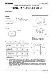
TC7SET17F/FU
2009-09-29
1
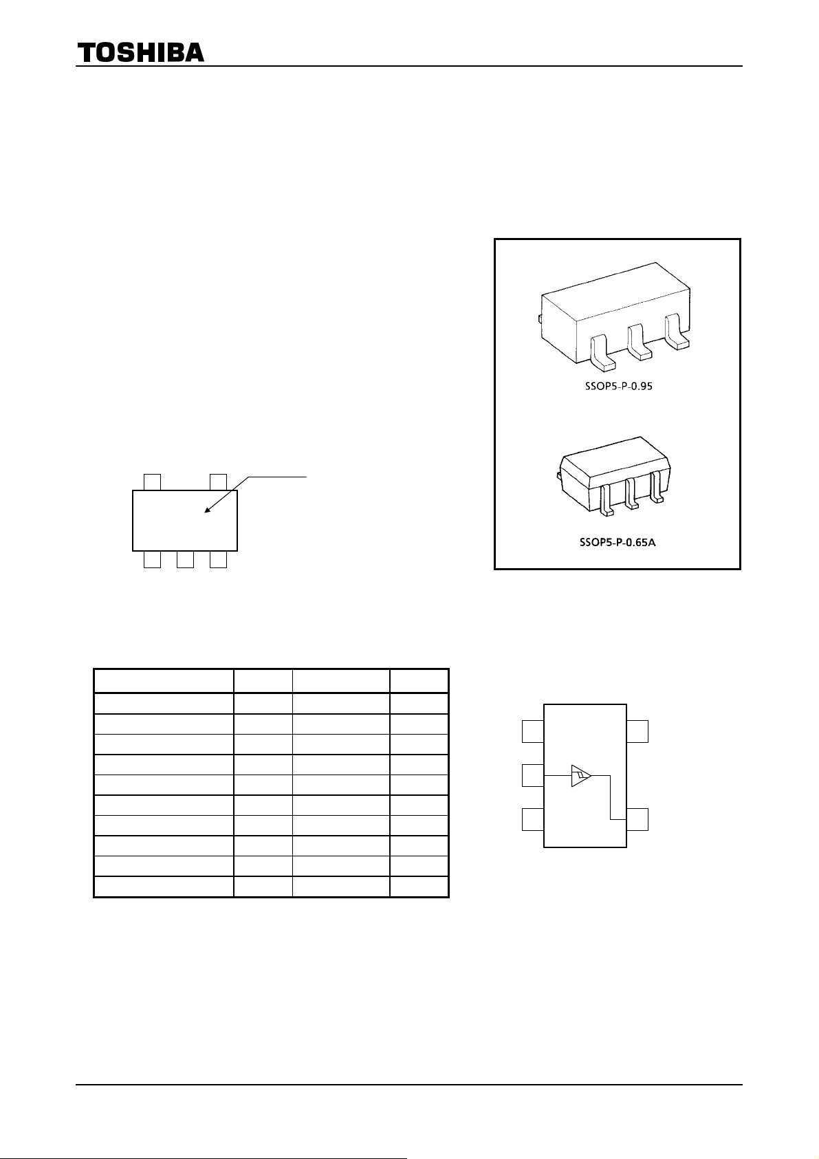
TOSHIBA CMOS Digital Integrated Circuit Silicon Monolithic
TC7SET17F,TC7SET17FU
Schmitt Buffer
Features
• High speed t
pd
= 5.0 ns (typ.)
at V
CC
= 5 V, C
L
= 15pF
• Low power dissipation I
CC
= 2 μA (max) at Ta = 25°C
• Compatible with TTL outputs.
• 5.5V tolerant input.
Marking
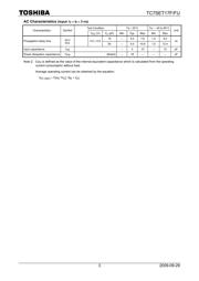
Absolute Maximum Ratings
(Ta
=
25°C)
Characteristics Symbol Rating Unit
Supply voltage V
CC
−0.5 to 7.0 V
DC input voltage V
IN
−0.5 to 7.0 V
DC output voltage V
OUT
−0.5 to V
CC
+ 0.5 V
Input diode current I
IK
−20 mA
Output diode current I
OK
±20 (Note 1) mA
DC output current I
OUT
±25 mA
DC V
CC
/ground current I
CC
±50 mA
Power dissipation P
D
200 mW
Storage temperature T
stg
−65 to 150 °C
Lead temperature (10 s) T
L
260 °C
Note: Using continuously under heavy loads (e.g. the application of high temperature/current/voltage and the
significant change in temperature, etc.) may cause this product to decrease in the reliability significantly
even if the operating conditions (i.e. operating temperature/current/voltage, etc.) are within the absolute
maximum ratings and the operating ranges.
Please design the appropriate reliability upon reviewing the Toshiba Semiconductor Reliability Handbook
(“Handling Precautions”/“Derating Concept and Methods”) and individual reliability data (i.e. reliability test
report and estimated failure rate, etc).
Note 1: V
OUT
< GND, V
OUT
> V
CC
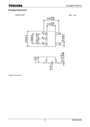
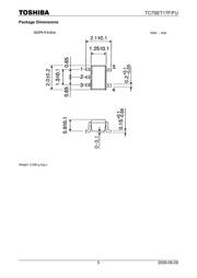
TC7SET17F
TC7SET17FU
Weight
SSOP5-P-0.95 : 0.016 g (typ.)
SSOP5-P-0.65A : 0.006 g (typ.)
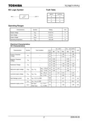
Pin Assignment
(top view)
Product name
G L
(
SMV
)
(USV)
GND 3
NC 1
IN A 2
5 V
CC
4 OUT Y
器件 Datasheet 文档搜索
AiEMA 数据库涵盖高达 72,405,303 个元件的数据手册,每天更新 5,000 多个 PDF 文件
