Datasheet 搜索 > 双极性晶体管 > ON Semiconductor(安森美) > TIP31BG 数据手册 > TIP31BG 其他数据使用手册 1/8 页

¥ 2.065
TIP31BG 其他数据使用手册 - ON Semiconductor(安森美)
制造商:
ON Semiconductor(安森美)
分类:
双极性晶体管
封装:
TO-220-3
描述:
ON SEMICONDUCTOR TIP31BG 射频双极晶体管
Pictures:
3D模型
符号图
焊盘图
引脚图
产品图
页面导航:
导航目录
TIP31BG数据手册
Page:
of 8 Go
若手册格式错乱,请下载阅览PDF原文件
© Semiconductor Components Industries, LLC, 2015
September, 2015 − Rev. 16
1 Publication Order Number:
TIP31A/D
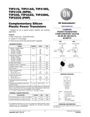
TIP31G, TIP31AG, TIP31BG,
TIP31CG (NPN),
TIP32G,TIP32AG, TIP32BG,
TIP32CG(PNP)
Complementary Silicon
Plastic Power Transistors
Designed for use in general purpose amplifier and switching
applications.
Features
• High Current Gain − Bandwidth Product
• Compact TO−220 Package
• These Devices are Pb−Free and are RoHS Compliant*
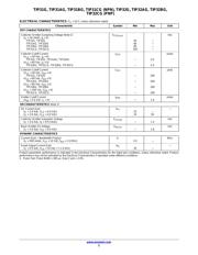
MAXIMUM RATINGS
Rating Symbol Value Unit
Collector − Emitter Voltage
TIP31G, TIP32G
TIP31AG, TIP32AG
TIP31BG, TIP32BG
TIP31CG, TIP32CG
V
CEO
40
60
80
100
Vdc
Collector−Base Voltage
TIP31G, TIP32G
TIP31AG, TIP32AG
TIP31BG, TIP32BG
TIP31CG, TIP32CG
V
CB
40
60
80
100
Vdc
Emitter−Base Voltage V
EB
5.0 Vdc
Collector Current − Continuous I
C
3.0 Adc
Collector Current − Peak I
CM
5.0 Adc
Base Current I
B
1.0 Adc
Total Power Dissipation
@ T
C
= 25°C
Derate above 25°C
P
D
40
0.32
W
W/°C
Total Power Dissipation
@ T
A
= 25°C
Derate above 25°C
P
D
2.0
0.016
W
W/°C
Unclamped Inductive Load Energy
(Note 1)
E 32 mJ
Operating and Storage Junction Tem-
perature Range
T
J
, T
stg
–65 to +150 °C
Stresses exceeding those listed in the Maximum Ratings table may damage the
device. If any of these limits are exceeded, device functionality should not be
assumed, damage may occur and reliability may be affected.
1. I
C
= 1.8 A, L = 20 mH, P.R.F. = 10 Hz, V
CC
= 10 V, R
BE
= 100 W
THERMAL CHARACTERISTICS
Characteristic Symbol Max Unit
Thermal Resistance, Junction−to−Ambient
R
q
JA
62.5 °C/W
Thermal Resistance, Junction−to−Case
R
q
JC
3.125 °C/W
*For additional information on our Pb−Free strategy and soldering details, please
download the ON Semiconductor Soldering and Mounting Techniques
Reference Manual, SOLDERRM/D.
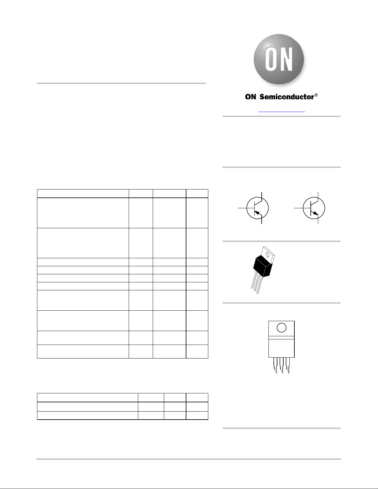
TO−220
CASE 221A
STYLE 1
MARKING DIAGRAM
3 AMPERE
POWER TRANSISTORS
COMPLEMENTARY SILICON
40−60−80−100 VOLTS,
40 WATTS
www.onsemi.com
1
2
3
4
TIP3xx = Device Code
xx = 1, 1A, 1B, 1C,
2, 2A, 2B, 2C,
A = Assembly Location
Y = Year
WW = Work Week
G Pb−Free Package
TIP3xxG
AYWW
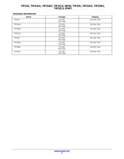
See detailed ordering and shipping information on page 6 o
f
this data sheet.
ORDERING INFORMATION
1
BASE
3
EMITTER
COLLECTOR
2,4
1
BASE
3
EMITTER
COLLECTOR
2,4
NPNPNP
器件 Datasheet 文档搜索
AiEMA 数据库涵盖高达 72,405,303 个元件的数据手册,每天更新 5,000 多个 PDF 文件
