Datasheet 搜索 > DSP数字信号处理器 > TI(德州仪器) > TMS320C5505AZCH10 数据手册 > TMS320C5505AZCH10 其他数据使用手册 6/21 页
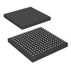
 器件3D模型
¥ 60.667
TMS320C5505AZCH10 其他数据使用手册 - TI(德州仪器)
制造商:
TI(德州仪器)
分类:
DSP数字信号处理器
封装:
LFBGA-196
描述:
TMS320C5505定点数字信号处理器 TMS320C5505 Fixed-Point Digital Signal Processor
Pictures:
3D模型
符号图
焊盘图
引脚图
产品图
页面导航:
技术参数、封装参数在P6P7P8P9
应用领域在P21
型号编号列表在P5
导航目录
TMS320C5505AZCH10数据手册
Page:
of 21 Go
若手册格式错乱,请下载阅览PDF原文件

Silicon Revision 2.0 Usage Notes and Known Design Exceptions to Functional Specifications
www.ti.com
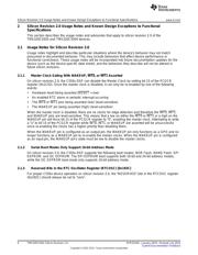
2 Silicon Revision 2.0 Usage Notes and Known Design Exceptions to Functional
Specifications
This section describes the usage notes and advisories that apply to silicon revision 2.0 of the
TMS320C5505 and TMS320C5504 devices.
2.1 Usage Notes for Silicon Revision 2.0
Usage notes highlight and describe particular situations where the device's behavior may not match
presumed or documented behavior. This may include behaviors that affect device performance or
functional correctness. These usage notes will be incorporated into future documentation updates for the
device (such as the device-specific data sheet), and the behaviors they describe will not be altered in
future silicon revisions.
2.1.1 Master Clock Gating With WAKEUP, INT0, or INT1 Asserted
On silicon revision 2.0, the C550x DSP can disable the Master Clock by setting bit 15 of the PCGCR
register (0x1C02). Once the master clock is disabled, it can only be re-enabled by one of the following
events:
• Hardware reset being asserted ( RESET = low)
• An enabled RTC alarm or periodic interrupt occurring
• The INT0 or INT1 pins being asserted (low) (level-sensitive)
• The WAKEUP pin being asserted (high) (level-sensitive)
When the master clock is disabled, there are no clocks for edge detection and therefore the INT0, INT1,
and WAKEUP pins are level-sensitive. This means that a low on either the INT0 or INT1 or a high on the
WAKEUP pin will force bit 15 of the PCGCR register to "0", enabling the master clock. Attempting to write
a "1" to bit 15 of the PCGCR register while INT0, INT1, or WAKEUP are asserted will be unsuccessful
since re-enabling the clocks has a higher priority than disabling them.
When the WAKEUP pin is configured as an output-pin, the WAKEUP pin only functions as a GPO and no
longer functions as a WAKEUP pin to re-enable the master clocks. When the WAKEUP pin is configured
as an input-pin, the WAKEUP pin's state must be low to disable the master clocks.
2.1.2 Serial Boot Modes Only Support 16-bit Address Mode
On silicon revision 2.0, the C550x DSP supports the following boot modes: NOR Flash, NAND Flash, SPI
EEPROM, and I2C EEPROM. The SPI EEPROM boot supports both 16-bit and 24-bit address modes,
while the I2C EEPROM boot mode only supports 16-bit address mode.
2.1.3 Reserved Bits in the RTC Oscillator Register (RTCOSC) [0x192C]
For proper C550x device operation on silicon revision 2.0, the "RESERVED" bits in the RTCOSC register
(0x192C) should always be set to "zero".
6
TMS320C550x Silicon Revision 2.0 SPRZ310D–January 2010–Revised July 2015
Submit Documentation Feedback
Copyright © 2010–2015, Texas Instruments Incorporated
器件 Datasheet 文档搜索
AiEMA 数据库涵盖高达 72,405,303 个元件的数据手册,每天更新 5,000 多个 PDF 文件
