Datasheet 搜索 > DC/DC转换器 > TI(德州仪器) > TPS40055PWPR 数据手册 > TPS40055PWPR 其他数据使用手册 3/42 页
 器件3D模型
¥ 6.786
TPS40055PWPR 其他数据使用手册 - TI(德州仪器)
制造商:
TI(德州仪器)
分类:
DC/DC转换器
封装:
HTSSOP-16
描述:
TEXAS INSTRUMENTS TPS40055PWPR 芯片, 直流/直流控制器, 同步降压, 1MHZ, HTSSOP-16 新
Pictures:
3D模型
符号图
焊盘图
引脚图
产品图
页面导航:
引脚图在P3Hot
典型应用电路图在P20P21P22P23P24P25
原理图在P8
封装尺寸在P32P34P35
标记信息在P32P33
封装信息在P29P32P33P34P35
技术参数、封装参数在P4
应用领域在P33
电气规格在P5P6P21
导航目录
TPS40055PWPR数据手册
Page:
of 42 Go
若手册格式错乱,请下载阅览PDF原文件
1
2
3
4
5
6
7
8
16
15
14
13
12
11
10
9
ILIM
VIN
BOOST
HDRV
SW
BP10
LDRV
PGND
KFF
RT
BP5
SYNC
SGND
SS/SD
VFB
COMP
Thermal Pad
3
TPS40054
,
TPS40055
,
TPS40057
www.ti.com.cn
ZHCSAK8I –DECEMBER 2003–REVISED DECEMBER 2014
Copyright © 2003–2014, Texas Instruments Incorporated
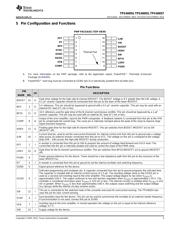
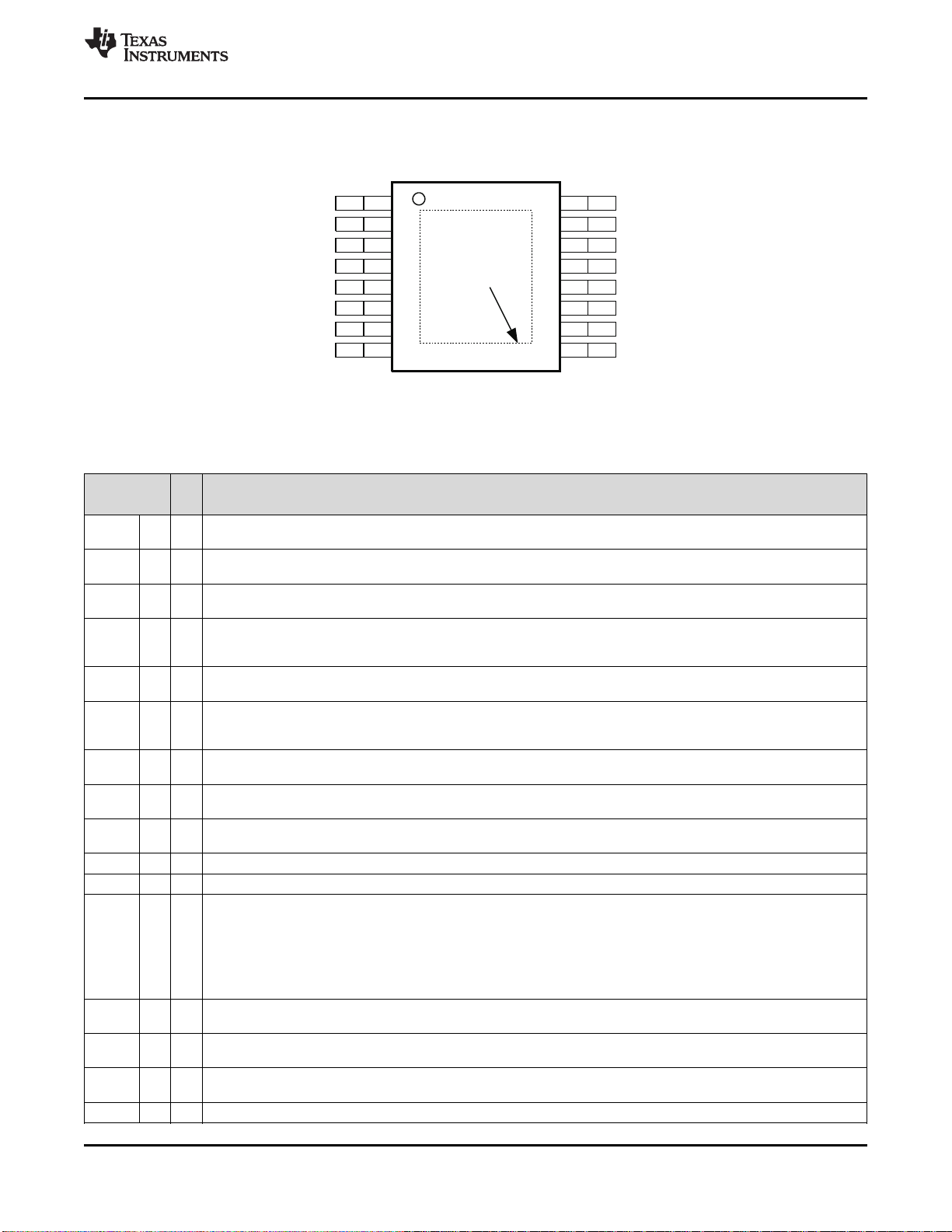
5 Pin Configuration and Functions
PWP PACKAGE (TOP VIEW)
A. For more information on the PWP package, refer to the application report, PowerPAD™ Thermally Enhanced
Package (SLMA002).
B. PowerPAD™ heat slug must be connected to SGND (pin 5) or electrically isolated from all other pins.
Pin Functions
PIN
I/O DESCRIPTION
NAME NO.
BOOST 14 O
Gate drive voltage for the high side N-channel MOSFET. The BOOST voltage is 9 V greater than the SW voltage. A
0.1-µF ceramic capacitor should be connected from this pin to the drain of the lower MOSFET.
BP5 3 O
5-V reference. This pin should be bypassed to ground with a 0.1-µF ceramic capacitor. This pin may be used with an
external DC load of 1 mA or less.
BP10 11 O
10-V reference used for gate drive of the N-channel synchronous rectifier. This pin should be bypassed by a 1-µF
ceramic capacitor. This pin may be used with an external DC load of 1 mA or less.
COMP 8 O
Output of the error amplifier, input to the PWM comparator. A feedback network is connected from this pin to the VFB
pin to compensate the overall loop. The comp pin is internally clamped above the peak of the ramp to improve large
signal transient response.
HDRV 13 O
Floating gate drive for the high-side N-channel MOSFET. This pin switches from BOOST (MOSFET on) to SW
(MOSFET off).
ILIM 16 I
Current limit pin, used to set the overcurrent threshold. An internal current sink from this pin to ground sets a voltage
drop across an external resistor connected from this pin to VCC. The voltage on this pin is compared to the voltage
drop (VIN – SW) across the high-side MOSFET during conduction.
KFF 1 I
A resistor is connected from this pin to VIN to program the amount of voltage feed-forward and UVLO level. The
current fed into this pin is internally divided and used to control the slope of the PWM ramp.
LDRV 10 O
Gate drive for the N-channel synchronous rectifier. This pin switches from BP10 (MOSFET on) to ground (MOSFET
off).
PGND 9
Power ground reference for the device. There should be a low-impedance path from this pin to the source(s) of the
lower MOSFET(s).
RT 2 I A resistor is connected from this pin to ground to set the internal oscillator and switching frequency.
SGND 5 Signal ground reference for the device.
SS/SD 6 I
Soft-start programming and shutdown pin. A capacitor connected from this pin to ground programs the soft-start time.
The capacitor is charged with an internal current source of 2.3 µA. The resulting voltage ramp on the SS/SD pin is
used as a second non-inverting input to the error amplifier. The output voltage begins to rise when V
SS/SD
is
approximately 0.85 V. The output continues to rise and reaches regulation when V
SS/SD
is approximately 1.55 V. The
controller is considered shut down when V
SS/SD
is 125 mV or less. The internal circuitry is enabled when V
SS/SD
is 210
mV or greater. When V
SS/SD
is less than approximately 0.85 V, the outputs cease switching and the output voltage
(V
O
) decays while the internal circuitry remains active.
SW 12 I
This pin is connected to the switched node of the converter and used for overcurrent sensing. The TPS40054 also
uses this pin for zero current sensing.
SYNC 4 I
Syncronization input for the device. This pin can be used to synchronize the oscillator to an external master frequency.
If synchronization is not used, connect this pin to SGND.
VFB 7 I
Inverting input to the error amplifier. In normal operation the voltage on this pin is equal to the internal reference
voltage, 0.7 V.
VIN 15 I Supply voltage for the device.
器件 Datasheet 文档搜索
AiEMA 数据库涵盖高达 72,405,303 个元件的数据手册,每天更新 5,000 多个 PDF 文件
