Datasheet 搜索 > FET驱动器 > TI(德州仪器) > UCC27201ADRMR 数据手册 > UCC27201ADRMR 其他数据使用手册 1/42 页
 器件3D模型
¥ 0.688
UCC27201ADRMR 其他数据使用手册 - TI(德州仪器)
制造商:
TI(德州仪器)
分类:
FET驱动器
封装:
VSON-8
描述:
120 -V启动, 3 - A峰值,高频率,高侧/低侧驱动器 120-V Boot, 3-A Peak, High Frequency, High-Side/Low-Side Driver
Pictures:
3D模型
符号图
焊盘图
引脚图
产品图
页面导航:
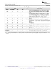
引脚图在P3P4Hot
典型应用电路图在P14P15
原理图在P12
封装尺寸在P23P24P25P26
标记信息在P23P24
封装信息在P22P23P24P25P26
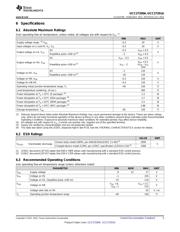
技术参数、封装参数在P5
应用领域在P1P42
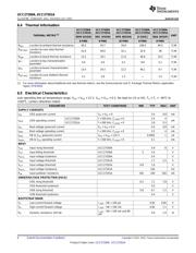
电气规格在P6P7
导航目录
UCC27201ADRMR数据手册
Page:
of 42 Go
若手册格式错乱,请下载阅览PDF原文件
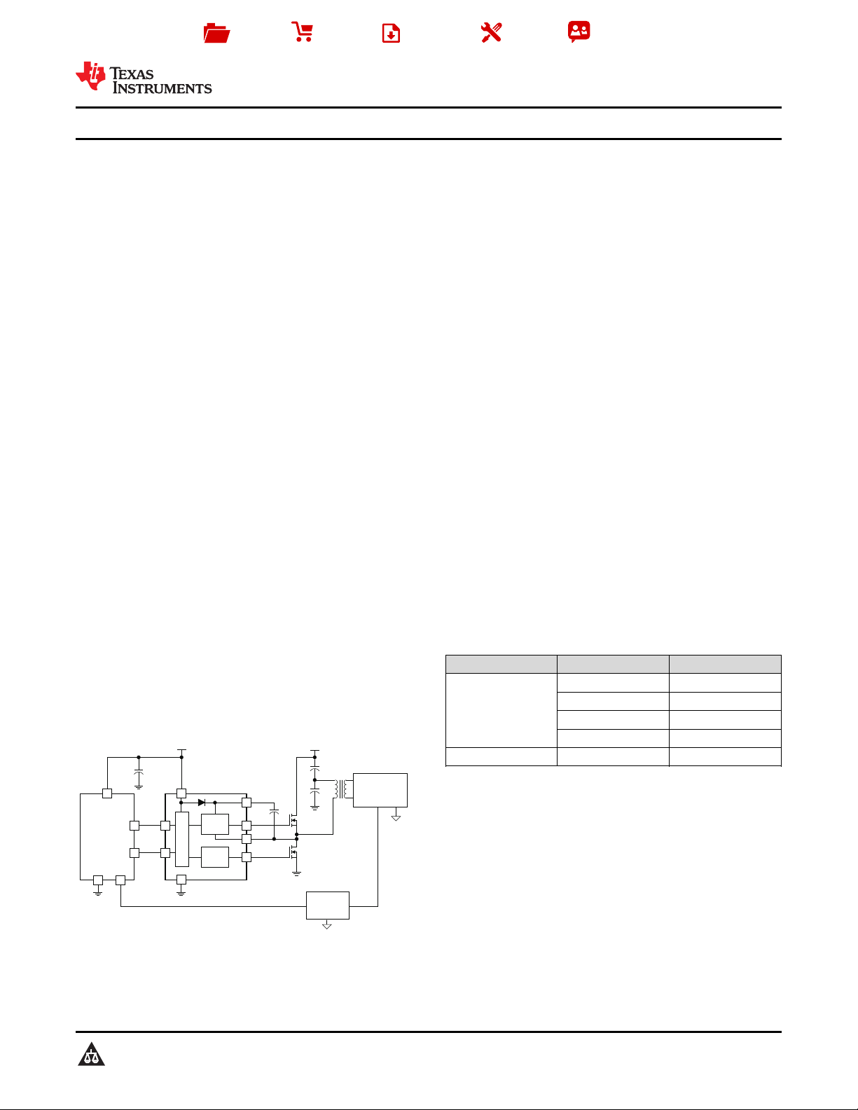
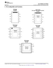
PWM
CONTROLLER
+12V
ISOLATION
AND
FEEDBACK
+100V
SECONDARY
SIDE
CIRCUIT
HI
CONTROL
DRIVE
LO
DRIVE
HI
V
DD
UCC27200A/1A
V
SS
LI
HB
HO
HS
LO
Product
Folder
Sample &
Buy
Technical
Documents
Tools &
Software
Support &
Community
UCC27200A
,
UCC27201A
SLUSAF9B –FEBRUARY 2011–REVISED JULY 2015
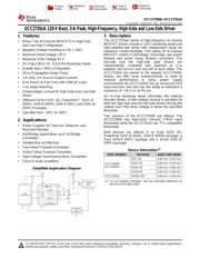
UCC2720xA 120-V Boot, 3-A Peak, High-Frequency, High-Side and Low-Side Driver
1 Features 3 Description
The UCC2720xA family of high-frequency N-channel
1
• Drives Two N-Channel MOSFETs in High-Side
MOSFET drivers include a 120-V bootstrap diode and
and Low-Side Configuration
high-side/low-side driver with independent inputs for
• Negative Voltage Handling on HS (–18V)
maximum control flexibility. This allows for N-channel
• Maximum Boot Voltage 120 V
MOSFET control in half-bridge, full-bridge, two-switch
forward and active clamp forward converters. The
• Maximum VDD Voltage 20 V
low-side and the high-side gate drivers are
• On-Chip 0.65-V VF, 0.6-Ω RD Bootstrap Diode
independently controlled and matched to 1-ns
• Greater than 1 MHz of Operation
between the turn-on and turn-off of each other. The
UCC2720xA are based on the popular UCC27200/1
• 20-ns Propagation Delay Times
drivers, but offer some enhancements. In order to
• 3-A Sink, 3-A Source Output Currents
improve performance in noisy power supply
• 8-ns Rise/7-ns Fall Time with 1000-pF Load
environments the UCC2720xA has an enhanced ESD
• 1-ns Delay Matching
input structure and also has the ability to withstand a
maximum of –18 V on its HS pin.
• Undervoltage Lockout for High-Side and Low-Side
Driver
An on-chip bootstrap diode eliminates the external
discrete diodes. Under-voltage lockout is provided for
• Offered in 8-Pin SOIC (D), PowerPAD™ SOIC-8
both the high-side and the low-side drivers forcing the
(DDA), SON-8 (DRM), SON-9 (DRC) and SON-10
outputs low if the drive voltage is below the specified
(DPR) Packages
threshold.
• Specified from –40°C to 140°C
Two versions of the UCC27200A are offered. The
UCC27200A has high-noise immune CMOS input
2 Applications
thresholds while the UCC27201A has TTL-compatible
• Power Supplies for Telecom, Datacom, and
thresholds.
Merchant Markets
Both devices are offered in an 8-pin SOIC (D),
• Half-Bridge Applications and Full-Bridge
PowerPad SOIC-8 (DDA), SON-8 (DRM) package, a
Converters
9-pin SON-9 (DRC) package and a 10-pin SON-10
• Isolated Bus Architecture
(DPR) package.
• Two-Switch Forward Converters
Device Information
(1)
• Active-Clamp Forward Converters
PART NUMBER PACKAGE BODY SIZE (NOM)
• High-Voltage Synchronous-Buck Converters
SOIC (8) 4.90 mm × 3.91 mm
• Class-D Audio Amplifiers
HSOP (8) 4.89 mm × 3.90 mm
UCC27200A,
UCC27201A
VSON (9) 3.00 mm × 3.00 mm
Simplified Application Diagram
VSON (8) 4.00 mm × 4.00 mm
UCC27201A WSON (10) 4.00 mm × 4.00 mm
(1) For all available packages, see the orderable addendum at
the end of the data sheet.
1
An IMPORTANT NOTICE at the end of this data sheet addresses availability, warranty, changes, use in safety-critical applications,
intellectual property matters and other important disclaimers. PRODUCTION DATA.
器件 Datasheet 文档搜索
AiEMA 数据库涵盖高达 72,405,303 个元件的数据手册,每天更新 5,000 多个 PDF 文件
