Datasheet 搜索 > FPGA芯片 > Xilinx(赛灵思) > XC2S50-5PQ208C 数据手册 > XC2S50-5PQ208C 产品描述及参数 1/4 页
 器件3D模型
¥ 224.138
XC2S50-5PQ208C 产品描述及参数 - Xilinx(赛灵思)
制造商:
Xilinx(赛灵思)
分类:
FPGA芯片
封装:
BFQFP-208
Pictures:
3D模型
符号图
焊盘图
引脚图
产品图
页面导航:
原理图在P2
型号编码规则在P1P2P3
导航目录
XC2S50-5PQ208C数据手册
Page:
of 4 Go
若手册格式错乱,请下载阅览PDF原文件
DS001-1 (v2.3) November 1, 2001 www.xilinx.com 1
Preliminary Product Specification 1-800-255-7778
© 2001 Xilinx, Inc. All rights reserved. All Xilinx trademarks, registered trademarks, patents, and disclaimers are as listed at http://www.xilinx.com/legal.htm.
All other trademarks and registered trademarks are the property of their respective owners. All specifications are subject to change without notice.
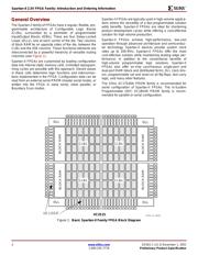
Introduction
The Spartan™-II 2.5V Field-Programmable Gate Array fam-
ily gives users high performance, abundant logic resources,
and a rich feature set, all at an exceptionally low price. The
six-member family offers densities ranging from 15,000 to
200,000 system gates, as shown in Table 1. System perfor-
mance is supported up to 200 MHz.
Spartan-II devices deliver more gates, I/Os, and features
per dollar than other FPGAs by combining advanced pro-
cess technology with a streamlined Virtex-based architec-
ture. Features include block RAM (to 56K bits), distributed
RAM (to 75,264 bits), 16 selectable I/O standards, and four
DLLs. Fast, predictable interconnect means that successive
design iterations continue to meet timing requirements.
The Spartan-II family is a superior alternative to
mask-programmed ASICs. The FPGA avoids the initial cost,
lengthy development cycles, and inherent risk of
conventional ASICs. Also, FPGA programmability permits
design upgrades in the field with no hardware replacement
necessary (impossible with ASICs).
Features
• Second generation ASIC replacement technology
- Densities as high as 5,292 logic cells with up to
200,000 system gates
- Streamlined features based on Virtex architecture
- Unlimited reprogrammability
- Very low cost
• System level features
- SelectRAM+™ hierarchical memory:
· 16 bits/LUT distributed RAM
· Configurable 4K bit block RAM
· Fast interfaces to external RAM
- Fully PCI compliant
- Low-power segmented routing architecture
- Full readback ability for verification/observability
- Dedicated carry logic for high-speed arithmetic
- Dedicated multiplier support
- Cascade chain for wide-input functions
- Abundant registers/latches with enable, set, reset
- Four dedicated DLLs for advanced clock control
- Four primary
low-skew global clock distribution nets
- IEEE 1149.1 compatible boundary scan logic
• Versatile I/O and packaging
- Low cost packages available in all densities
- Family footprint compatibility in common packages
- 16 high-performance interface standards
- Hot swap Compact PCI friendly
- Zero hold time simplifies system timing
• Fully supported by powerful Xilinx development system
- Foundation ISE Series: Fully integrated software
- Alliance Series: For use with third-party tools
- Fully automatic mapping, placement, and routing
0
Spartan-II 2.5V FPGA Family:
Introduction and Ordering
Information
DS001-1 (v2.3) November 1, 2001
00
Preliminary Product Specification
R
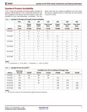
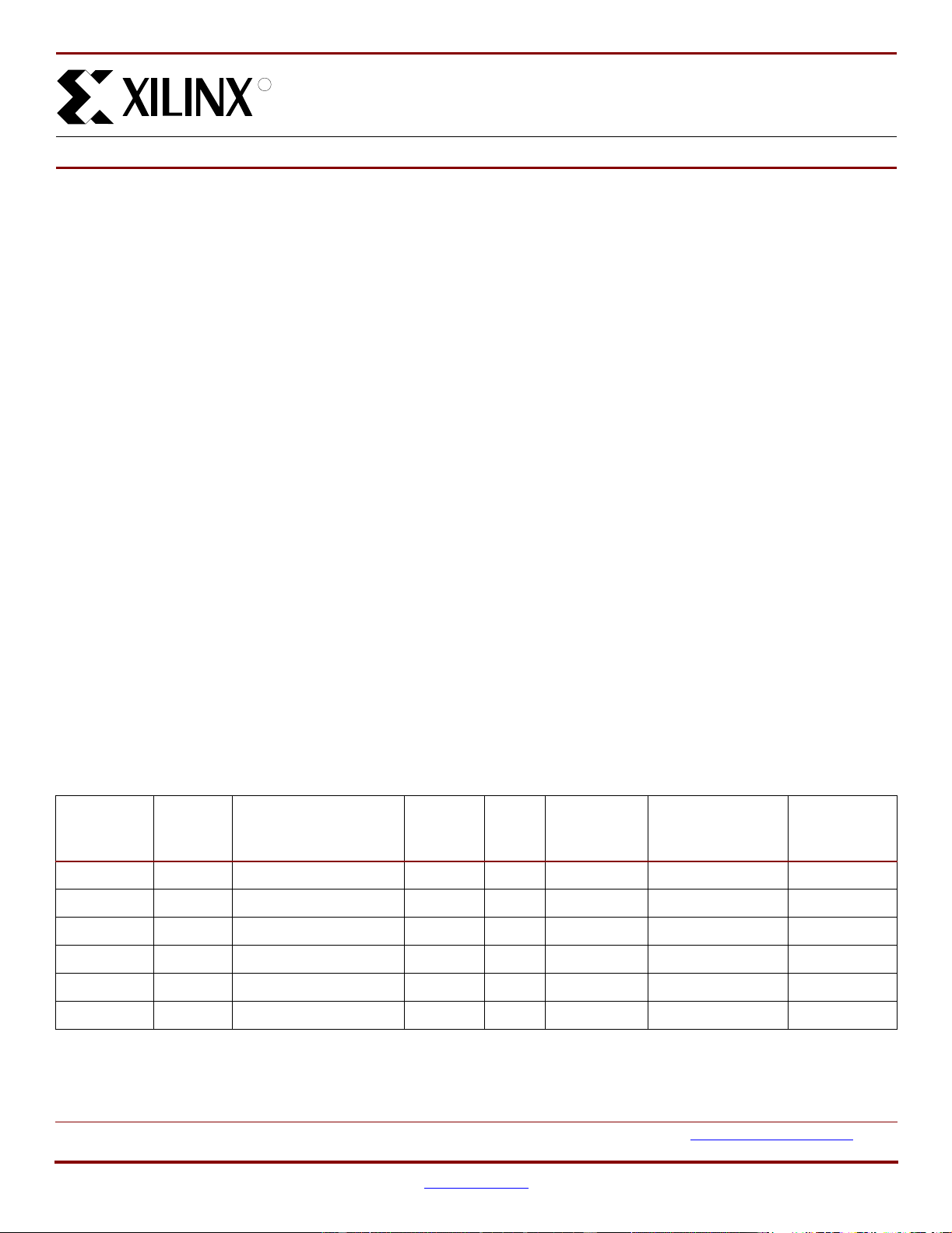
Table 1: Spartan-II FPGA Family Members
Device
Logic
Cells
System Gates
(Logic and RAM)
CLB
Array
(R x C)
Total
CLBs
Maximum
Available
User I/O
(1)
Total
Distributed RAM
Bits
Total
Block RAM
Bits
XC2S15 432 15,000 8 x 12 96 86 6,144 16K
XC2S30 972 30,000 12 x 18 216 132 13,824 24K
XC2S50 1,728 50,000 16 x 24 384 176 24,576 32K
XC2S100 2,700 100,000 20 x 30 600 196 38,400 40K
XC2S150 3,888 150,000 24 x 36 864 260 55,296 48K
XC2S200 5,292 200,000 28 x 42 1,176 284 75,264 56K
Notes:
1. All user I/O counts do not include the four global clock/user input pins. See details in Table 3, page 3.
器件 Datasheet 文档搜索
AiEMA 数据库涵盖高达 72,405,303 个元件的数据手册,每天更新 5,000 多个 PDF 文件
