Datasheet 搜索 > EEPROM芯片 > Xilinx(赛灵思) > XCF08PVOG48C 数据手册 > XCF08PVOG48C 其他数据使用手册 5/42 页

 器件3D模型
¥ 224.953
XCF08PVOG48C 其他数据使用手册 - Xilinx(赛灵思)
制造商:
Xilinx(赛灵思)
分类:
EEPROM芯片
封装:
TSOP-48
描述:
XILINX XCF08PVOG48C 芯片, 存储器, PROM, 闪存平台, 8Mb, 48TSOP
Pictures:
3D模型
符号图
焊盘图
引脚图
产品图
页面导航:

导航目录
XCF08PVOG48C数据手册
Page:
of 42 Go
若手册格式错乱,请下载阅览PDF原文件
Platform Flash In-System Programmable Configuration PROMS
DS123 (v2.6) March 14, 2005 www.xilinx.com 5
Preliminary Product Specification
R
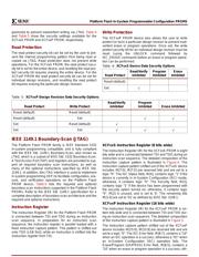
grammed to prevent inadvertent writing via JTAG. Table 4
and Table 5 show the security settings available for the
XCFxxS PROM and XCFxxP PROM, respectively.
Read Protection
The read protect security bit can be set by the user to pre-
vent the internal programming pattern from being read or
copied via JTAG. Read protection does not prevent write
operations. For the XCFxxS PROM, the read protect secu-
rity bit is set for the entire device, and resetting the read pro-
tect security bit requires erasing the entire device. For the
XCFxxP PROM the read protect security bit can be set for
individual design revisions, and resetting the read protect
bit requires erasing the particular design revision.
Write Protection
The XCFxxP PROM device also allows the user to write
protect (or lock) a particular design revision to prevent inad-
vertent erase or program operations. Once set, the write
protect security bit for an individual design revision must be
reset (using the UNLOCK command followed by
ISC_ERASE command) before an erase or program opera-
tion can be performed.
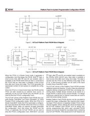
IEEE 1149.1 Boundary-Scan (JTAG)
The Platform Flash PROM family is IEEE Standard 1532
in-system programming compatible, and is fully compliant
with the IEEE Std. 1149.1 Boundary-Scan, also known as
JTAG, which is a subset of IEEE Std. 1532 Boundary-Scan.
A Test Access Port (TAP) and registers are provided to sup-
port all required boundary scan instructions, as well as
many of the optional instructions specified by IEEE Std.
1149.1. In addition, the JTAG interface is used to implement
in-system programming (ISP) to facilitate configuration, era-
sure, and verification operations on the Platform Flash
PROM device. Table 6 lists the required and optional
boundary-scan instructions supported in the Platform Flash
PROMs. Refer to the IEEE Std. 1149.1 specification for a
complete description of boundary-scan architecture and the
required and optional instructions.
Instruction Register
The Instruction Register (IR) for the Platform Flash PROM
is connected between TDI and TDO during an instruction
scan sequence. In preparation for an instruction scan
sequence, the instruction register is parallel loaded with a
fixed instruction capture pattern. This pattern is shifted out
onto TDO (LSB first), while an instruction is shifted into the
instruction register from TDI.
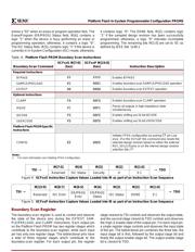
XCFxxS Instruction Register (8 bits wide)
The Instruction Register (IR) for the XCFxxS PROM is eight
bits wide and is connected between TDI and TDO during an
instruction scan sequence. The detailed composition of the
instruction capture pattern is illustrated in Figure 4. The
instruction capture pattern shifted out of the XCFxxS device
includes IR[7:0]. IR[7:5] are reserved bits and are set to a
logic "0". The ISC Status field, IR[4], contains logic "1" if the
device is currently in In-System Configuration (ISC) mode;
otherwise, it contains logic "0". The Security field, IR[3],
contains logic "1" if the device has been programmed with
the security option turned on; otherwise, it contains logic
"0". IR[2] is unused, and is set to '0'. The remaining bits
IR[1:0] are set to '01' as defined by IEEE Std. 1149.1.
XCFxxP Instruction Register (16 bits wide)
The Instruction Register (IR) for the XCFxxP PROM is six-
teen bits wide and is connected between TDI and TDO dur-
ing an instruction scan sequence. The detailed composition
of the instruction capture pattern is illustrated in Figure 5.
The instruction capture pattern shifted out of the XCFxxP
device includes IR[15:0]. IR[15:9] are reserved bits and are
set to a logic "0". The ISC Error field, IR[8:7], contains a "10"
when an ISC operation is a success; otherwise a "01" when
an In-System Configuration (ISC) operation fails. The
Erase/Program (ER/PROG) Error field, IR[6:5], contains a
"10" when an erase or program operation is a success; oth-
Table 4: XCFxxS Device Data Security Options
Read Protect
Read/Verify
Inhibited
Program
Inhibited
Erase
Inhibited
Reset (default)
Set
√
Table 5: XCFxxP Design Revision Data Security Options
Read Protect Write Protect
Read/Verify
Inhibited
Program
Inhibited Erase Inhibited
Reset (default) Reset (default)
Reset (default) Set
√√
Set Reset (default)
√
Set Set
√√√
器件 Datasheet 文档搜索
AiEMA 数据库涵盖高达 72,405,303 个元件的数据手册,每天更新 5,000 多个 PDF 文件
