Datasheet 搜索 > 微处理器 > Zilog > Z8S18020FEG 数据手册 > Z8S18020FEG 产品描述及参数 1/71 页
 器件3D模型
¥ 56.499
Z8S18020FEG 产品描述及参数 - Zilog
制造商:
Zilog
分类:
微处理器
封装:
QFP-80
描述:
Z8S180 系列 8 位 5 V 20 MHz 表面贴装 微控制器 - QFP-80
Pictures:
3D模型
符号图
焊盘图
引脚图
产品图
页面导航:
封装尺寸在P26
型号编码规则在P26
封装信息在P1
导航目录
Z8S18020FEG数据手册
Page:
of 71 Go
若手册格式错乱,请下载阅览PDF原文件
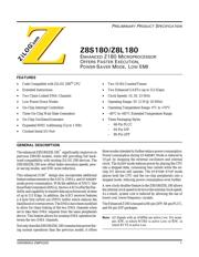
&5</2
24'.+/+0#4;241&7%652'%+(+%#6+10
<5<.
'0*#0%'&</+%41241%'5514
1(('45(#56'4':'%76+10
219'45#8'4/1&'.19'/+
('#674'5
Code Compatible with ZiLOG Z80
®
CPU
Extended Instructions
Two Chain-Linked DMA Channels
Low Power-Down Modes
On-Chip Interrupt Controllers
Three On-Chip Wait-State Generators
On-Chip Oscillator/Generator
Expanded MMU Addressing (Up to 1 MB)
Clocked Serial I/O Port
Two 16-Bit Counter/Timers
Two Enhanced UARTs (up to 512 Kbps)
Clock Speeds: 10, 20, 33 MHz
Operating Range: 5V (3.3V@ 20 MHz)
Operating Temperature Range: 0°C to +70°C
–40°C to +85°C Extended Temperature Range
Three Packaging Styles
– 68-Pin PLCC
–64-Pin DIP
–80-Pin QFP
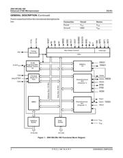
)'0'4#.&'5%4+26+10
The enhanced Z8S180/Z8L180
™
significantly improves on
previous Z80180 models, while still providing full back-
ward compatibility with existing ZiLOG Z80 devices. The
Z8S180/Z8L180 now offers faster execution speeds, pow-
er-saving modes, and EMI noise reduction.
This enhanced Z180
™
design also incorporates additional
feature enhancements to the ASCIs, DMAs, and
56#0&$;
mode power consumption. With the addition of ESCC-like
Baud Rate Generators (BRGs), the two ASCIs offer the flex-
ibility and capability to transfer data asynchronously at rates
of up to 512 Kbps. In addition, the ASCI receiver features
a 4-byte first in/first out (FIFO) buffer which reduces the
likelihood of overrun errors. The DMAs have been modified
to allow for chain-linking of the two DMA channels when
set to take their DMA requests from the same peripherals
device. This feature allows for nonstop DMA operation be-
tween the two DMA channels.
Not only does the Z8S180/Z8L180 consume less power dur-
ing normal operations than the previous model, it offers
three modes intended to further reduce power consumption.
Power consumption during
56#0&$; Mode is reduced to
10
µ
A by stopping the external oscillators and internal
clock. The
5.''2 mode reduces power by placing the CPU
into a stopped state, consuming less current while the on-
chip I/O devices still operate. The
5;56'/5612 mode
places both the CPU and the on-chip peripherals into a
stopped mode, reducing power consumption even further.
A new clock-doubler feature in the Z8S180/Z8L180 allows
the internal clock speed to be twice the external clock speed.
As a result, system cost is reduced by allowing the use of
lower-cost, lower-frequency crystals.
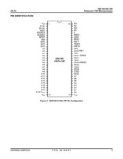
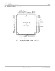
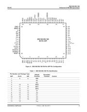
The Enhanced Z180 is housed in 80-pin QFP, 68-pin PLCC,
and 64-pin DIP packages.
0QVG All Signals with an overline are active Low. For exam-
ple: B/W
, in which WORD is active Low; or B/W, in
which BYTE is active Low.
器件 Datasheet 文档搜索
AiEMA 数据库涵盖高达 72,405,303 个元件的数据手册,每天更新 5,000 多个 PDF 文件
