Datasheet 搜索 > DA转换器 > ADI(亚德诺) > AD5666BRUZ-2 数据手册 > AD5666BRUZ-2 产品设计参考手册 6/29 页
 器件3D模型
¥ 71.43
AD5666BRUZ-2 产品设计参考手册 - ADI(亚德诺)
制造商:
ADI(亚德诺)
分类:
DA转换器
封装:
TSSOP-14
描述:
ANALOG DEVICES AD5666BRUZ-2 数模转换器, 四路, 16 bit, 95 kSPS, 串行, 2.7V 至 3.6V, 4.5V 至 5.5V, TSSOP, 14 引脚
Pictures:
3D模型
符号图
焊盘图
引脚图
产品图
页面导航:
导航目录
AD5666BRUZ-2数据手册
Page:
of 29 Go
若手册格式错乱,请下载阅览PDF原文件

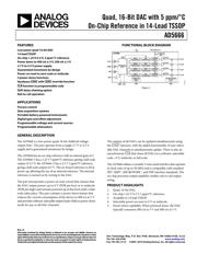
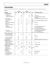
AD5666
Rev. D | Page 5 of 28
V
DD
= 2.7 V to 3.6 V, R
L
= 2 kΩ to GND, C
L
= 200 pF to GND, V
REFIN
= V
DD
. All specifications T
MIN
to T
MAX
, unless otherwise noted.
Table 2.
A Grade
1
B Grade
1
Parameter Min Typ Max Min Typ Max Unit Conditions/Comments
STATIC PERFORMANCE
2
Resolution 16 16 Bits
Relative Accuracy ±32 ±16 LSB See Figure 5
Differential Nonlinearity ±1 ±1 LSB
Guaranteed monotonic by design (see Figure
6)
Zero-Code Error 1 9 1 9 mV All 0s loaded to DAC register (see Figure 13)
Zero-Code Error Drift ±2 ±2 µV/°C
Full-Scale Error −0.2 −1 −0.2 −1 % FSR All 1s loaded to DAC register (see Figure 12)
Gain Error ±1 ±1 % FSR
Gain Temperature
Coefficient
±2.5 ±2.5 ppm Of FSR/°C
Offset Error ±1 ±9 ±1 ±9 mV
DC Power Supply Rejection
Ratio
–80 –80 dB V
DD
± 10%
DC Crosstalk
(External Reference)
10 10 µV
Due to full-scale output change,
R
L
= 2 kΩ to GND or V
DD
5 5 µV/mA Due to load current change
10 10 µV Due to powering down (per channel)
DC Crosstalk
(Internal Reference)
25 25 µV
Due to full-scale output change,
R
L
= 2 kΩ to GND or V
DD
10 10 µV/mA Due to load current change
OUTPUT CHARACTERISTICS
3
Output Voltage Range 0 V
DD
0 V
DD
V
Capacitive Load Stability 2 2 nF R
L
= ∞
10 10 nF R
L
= 2 kΩ
DC Output Impedance 0.5 0.5 Ω
Short-Circuit Current 30 30 mA V
DD
= 3 V coming out of power-down mode
Power-Up Time 4 4 s Coming out of power-down V
DD
= 3 V
REFERENCE INPUTS
Reference Input Voltage V
DD
V
DD
V
Reference Current 40 55 40 55 µA V
REF
= V
DD
= 3.6 V
Reference Input Range 0 V
DD
0 V
DD
Reference Input Impedance 14.6 14.6 kΩ Per DAC channel
REFERENCE OUTPUT
Output Voltage 1.247 1.253 1.247 1.253 V At ambient
Reference TC
3
±5 ±15 ±5 ±15 ppm/°C
Reference Output
Impedance
7.5 7.5 kΩ
LOGIC INPUTS
3
Input Current ±3 ±3 µA
Input Low Voltage, V
INL
0.8 0.8 V V
DD
= 3 V
Input High Voltage, V
INH
2 2 V V
DD
= 3 V
Pin Capacitance 3 3 pF
LOGIC OUTPUTS (SDO)
3
Output Low Voltage, V
OL
0.4 0.4 V I
SINK
= 2 mA
Output High Voltage, V
OH
V
DD
−
0.5
V
DD
−
0.5
I
SOURCE
= 2 mA
High Impedance Leakage
Current
±0.25 ±0.25 A
High Impedance Leakage
2 2 pF
器件 Datasheet 文档搜索
AiEMA 数据库涵盖高达 72,405,303 个元件的数据手册,每天更新 5,000 多个 PDF 文件
