Datasheet 搜索 > DA转换器 > ADI(亚德诺) > AD5676RBCPZ-REEL7 数据手册 > AD5676RBCPZ-REEL7 产品设计参考手册 1/34 页
 器件3D模型
¥ 42.018
AD5676RBCPZ-REEL7 产品设计参考手册 - ADI(亚德诺)
制造商:
ADI(亚德诺)
分类:
DA转换器
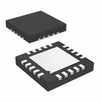
封装:
WFQFN-20
Pictures:
3D模型
符号图
焊盘图
引脚图
产品图
页面导航:
引脚图在P12P33Hot
典型应用电路图在P9
原理图在P1P24
封装尺寸在P33
型号编码规则在P34
焊接温度在P11
功能描述在P1P12P33
技术参数、封装参数在P1P3P5P9P11
应用领域在P1P31
电气规格在P13
导航目录
AD5676RBCPZ-REEL7数据手册
Page:
of 34 Go
若手册格式错乱,请下载阅览PDF原文件
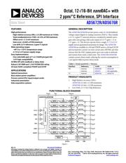
Octal, 12-/16-Bit nanoDAC+ with
2 ppm/°C Reference, SPI Interface
Data Sheet
AD5672R/AD5676R
Rev. B Document Feedback
Information furnished by Analog Devices is believed to be accurate and reliable. However, no
responsibility is assumed by Analog Devices for its use, nor for any infringements of patents or other
rights of third parties that may result from its use. Specifications subject to change without notice. No
license is granted by implication or otherwise under any patent or patent rights of Analog Devices.
Trademarks and registered trademarks are the property of their respective owners.
One Technology Way, P.O. Box 9106, Norwood, MA 02062-9106, U.S.A.
Tel: 781.329.4700 ©2014–2015 Analog Devices, Inc. All rights reserved.
Technical Support www.analog.com
FEATURES
High performance
High relative accuracy (INL): ±3 LSB maximum at 16 bits
Total unadjusted error (TUE): ±0.14% of FSR maximum
Offset error: ±1.5 mV maximum
Gain error: ±0.06% of FSR maximum
Low drift 2.5 V reference: 2 ppm/°C typical
Wide operating ranges
−40°C to +125°C temperature range
2.7 V to 5.5 V power supply range
Easy implementation
User selectable gain of 1 or 2 (GAIN pin/gain bit)
1.8 V logic compatibility
50 MHz SPI with readback or daisy chain
Robust 2 kV HBM and 1.5 kV FICDM ESD rating
20-lead, RoHS-compliant TSSOP and LFCSP
APPLICATIONS
Optical transceivers
Base station power amplifiers
Process control (PLC input/output cards)
Industrial automation
Data acquisition systems
GENERAL DESCRIPTION
The AD5672R/AD5676R are low power, octal, 12-/16-bit buffered
voltage output digital-to-analog converters (DACs). They include
a 2.5 V, 2 ppm/°C internal reference (enabled by default) and a
gain select pin giving a full-scale output of 2.5 V (gain = 1) or
5 V (gain = 2). The devices operate from a single 2.7 V to 5.5 V
supply and are guaranteed monotonic by design. The AD5672R/
AD5676R are available in a 20-lead TSSOP and in a 20-lead LFCSP
and incorporate a power-on reset circuit and a RSTSEL pin that
ensures that the DAC outputs power up to zero scale or midscale
and remain there until a valid write. The AD5672R/AD5676R
contain a power-down mode, reducing the current consumption to
1 µA typical while in power-down mode.
Table 1. Octal nanoDAC+® Devices
Interface Reference 16-Bit 12-Bit
SPI Internal AD5676R AD5672R
External AD5676 Not applicable
I
2
C Internal AD5675R AD5671R
PRODUCT HIGHLIGHTS
1. High Relative Accuracy (INL).
AD5672R (12-bit): ±1 LSB maximum.
AD5676R (16-bit): ±3 LSB maximum.
2. Low Drift, 2.5 V On-Chip Reference.
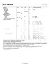
FUNCTIONAL BLOCK DIAGRAM
INTERFACE LOGIC
INPUT
REGISTER
SDO
SDI
GND
V
OUT
7
LDAC
SYNC
SCLK
AD5672R/AD5676R
RESET
2.5V
REF
V
OUT
0
V
OUT
1
V
OUT
2
V
OUT
3
V
OUT
4
V
OUT
5
V
OUT
6
DAC
REGISTER
STRING
DAC 0
BUFFER
INPUT
REGISTER
DAC
REGISTER
STRING
DAC 1
BUFFER
INPUT
REGISTER
DAC
REGISTER
STRING
DAC 2
BUFFER
INPUT
REGISTER
DAC
REGISTER
STRING
DAC 3
BUFFER
INPUT
REGISTER
DAC
REGISTER
STRING
DAC 4
BUFFER
INPUT
REGISTER
DAC
REGISTER
STRING
DAC 5
BUFFER
INPUT
REGISTER
DAC
REGISTER
STRING
DAC 6
BUFFER
INPUT
REGISTER
DAC
REGISTER
STRING
DAC 7
BUFFER
GAIN
POWER-DOWN
LOGIC
POWER-ON
RESET
11954-001
V
LOGIC
V
DD
V
REFOUT
RSTSEL
GAIN
×1/×2
Figure 1.
器件 Datasheet 文档搜索
AiEMA 数据库涵盖高达 72,405,303 个元件的数据手册,每天更新 5,000 多个 PDF 文件
